Bismuth iodine cluster hybrid semiconductor perovskite material based on 1-butyl-4-methylpyridinium cation

A technology of methyl pyridinium cation and perovskite material, applied in semiconductor devices, semiconductor/solid-state device manufacturing, organic chemistry, etc., can solve problems such as large band gap, achieve moderate band gap, improve light absorption performance, Ease of purification

Pending Publication Date: 2022-04-19
CHINA JILIANG UNIV
View PDF0 Cites 0 Cited by
  • Summary
  • Abstract
  • Description
  • Claims
  • Application Information

AI Technical Summary

Problems solved by technology

However, the current band gap of such materials is too large to meet the needs of practical applications.

Method used


Image

  • Bismuth iodine cluster hybrid semiconductor perovskite material based on 1-butyl-4-methylpyridinium cation
  • Bismuth iodine cluster hybrid semiconductor perovskite material based on 1-butyl-4-methylpyridinium cation
  • Bismuth iodine cluster hybrid semiconductor perovskite material based on 1-butyl-4-methylpyridinium cation

Examples


Embodiment 1

[0027] Bulk perovskite-like materials (BMPY) 3 (Bi 2 I 9 ) Preparation of powder sample: Weigh 117.9mg (0.2mmol) of BiI 3 , 83mg (0.5mmol) of KI, 92.8mg (0.5mmol) of 1-butyl-4-methylpyridinium chloride; respectively dissolved in 5ml of acetonitrile and mixed in sequence, fully stirred to make it fully react, to obtain a reddish-brown color The solution was clarified; the above solution was rotary evaporated under reduced pressure at 35°C to remove all solvents, washed with water and ethanol several times, and then dried to obtain a reddish-brown powder product with a yield of 83%.

Embodiment 2

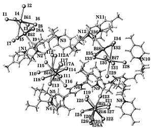
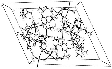
[0029] Synthetic perovskite-like materials (BMPY) 3 (Bi 2 I9 ) single crystal: Weigh 117.9mg (0.2mmol) of BiI 3 , 83mg (0.5mmol) of KI, 92.8mg (0.5mmol) of 1-butyl-4-methylpyridinium chloride; respectively dissolved in 5ml of acetonitrile and mixed in turn, fully stirred to fully react to obtain a reddish-brown color The solution was clarified; after filtration, the upper layer of the solution was covered with n-hexane to promote the crystallization of the product, and after standing for a few days, a large number of reddish-brown block crystals were precipitated. A reddish-brown bulk crystal with a size of 0.18mm×0.05mm×0.04mm was selected for X-ray single crystal structure test. The molecular structure of the compound is shown in the attached figure 1 , and its unit cell packing structure is shown in the attached figure 2 .

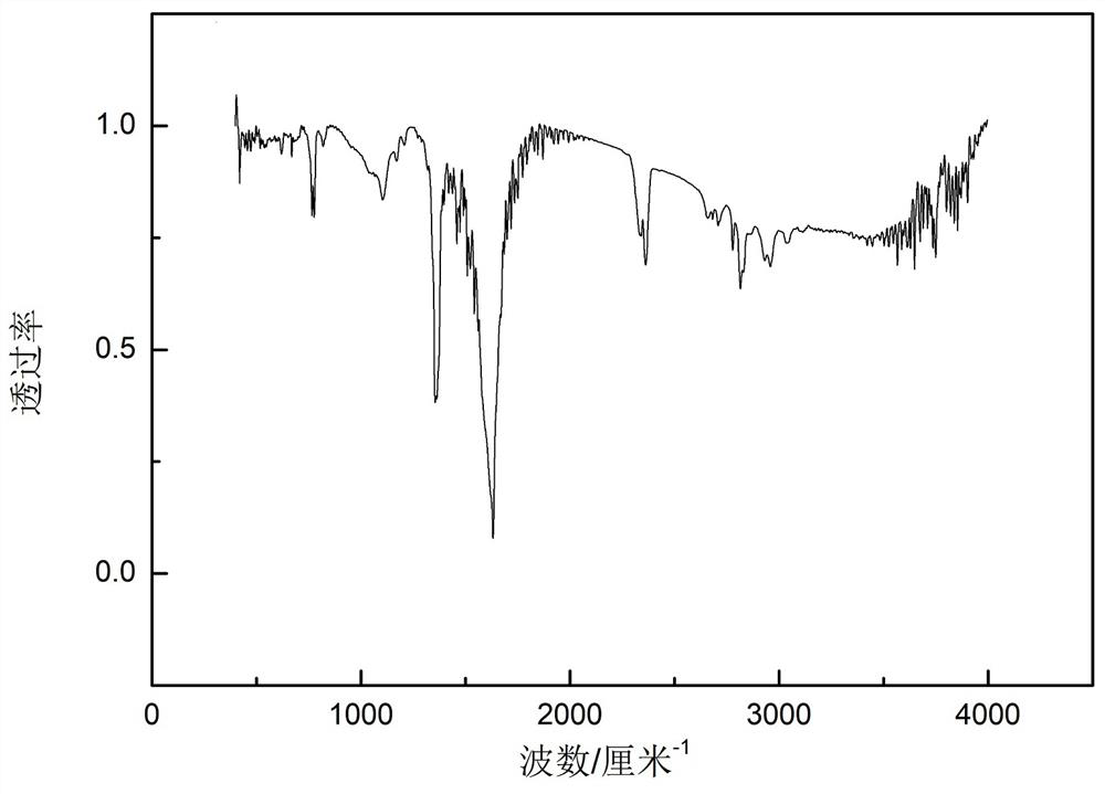
[0030] Pair of perovskite-like materials (BMPY) 3 (Bi 2 I 9 ) of the pure-phase powder samples were subjected to a series of performance tests...


PUM

PropertyMeasurementUnit
band gapaaaaaaaaaa

Abstract

The invention discloses a bismuth iodine cluster hybrid perovskite-like material based on a 1-butyl-4-methylpyridinium cation and a preparation method of the bismuth iodine cluster hybrid perovskite-like material. The perovskite-like compound hybrid material is synthesized from 1-butyl-4-methyl pyridine chloride, bismuth iodide and potassium iodide, the molecular structure of the perovskite-like compound hybrid material is (BMPY) 3 (Bi2I9), and in the formula, BMPY is a 1-butyl-4-methylpyridinium cation. The hybrid semiconductor material is a perovskite-like semiconductor material with moderate forbidden band width and good photoelectric response effect, and DFT calculation shows that the hybrid semiconductor material is a charge transfer salt. The material has the advantages of being cheap, completely free of lead and easy to purify, and has good solubility and stability. The material can be used as a semiconductor material in a halide-based perovskite photoelectric device.

Description

technical field [0001] The invention relates to the technical field of organic-inorganic hybrid materials and photoelectric materials, especially the technical field of hybrid semiconductor photoelectric materials. Background technique [0002] Perovskite-type organic-inorganic hybrid materials have been reported for a long time, but in recent years because of their unique structural composition and electronic (band) structure, especially their excellent performance in electronics, optics, and new energy, they have become a research topic. hotspot. Since the publication of the first work, a new generation of organic-inorganic hybrid perovskite solar cells has quickly demonstrated very high photoelectric conversion efficiency (>25%), and it also has the advantages of low material cost and simple fabrication process. , is considered to be the most promising new-generation photovoltaic technology, and is expected to become a sustainable new energy source in the future. Man...

Claims


Application Information

Patent Timeline
Patent Type & Authority Applications(China)
IPC IPC(8): C07D213/20C07D213/127H01L51/46
CPCC07D213/20C07D213/127C07B2200/13H10K85/654Y02E10/549
Inventor 柴文祥王友裕宋莉
Owner CHINA JILIANG UNIV
Why Eureka
Try Eureka