Method for cleaning pollutants on surface of silicon carbide wafer

A silicon carbide and pollutant technology, which is applied in chemical instruments and methods, cleaning methods and utensils, and cleaning methods using liquids, etc., can solve problems such as small accumulation of experience, no unified cleaning process, and late start of cleaning process.

Active Publication Date: 2011-02-23
BEIJING TIANKE HEDA SEMICON CO LTD
View PDF6 Cites 20 Cited by
  • Summary
  • Abstract
  • Description
  • Claims
  • Application Information

AI Technical Summary

Problems solved by technology

[0004] Since the cleaning process of silicon carbide wafers includes complex processes such as the removal of organic matter, inorganic matter, and oxide layers on the surface, and the exploration of the cleani...

Method used


Image

  • Method for cleaning pollutants on surface of silicon carbide wafer
  • Method for cleaning pollutants on surface of silicon carbide wafer
  • Method for cleaning pollutants on surface of silicon carbide wafer

Examples


Embodiment 1

[0021] Embodiment 1: cleaning of general silicon carbide wafer surface

[0022] First, make a mixed solution of acetone and ethanol according to the ratio of 3:1, and heat to 50°C. During the cleaning process, place 3 cups of the above-mentioned hot mixed solution, soak the silicon carbide wafer in each cup of solution for 3 minutes, and clean in turn. After cleaning 6 wafers, replace the first cup of turbid solution, the remaining three cups in sequence, and replace the last cup with a new clean mixed solution. After washing 3 silicon carbide wafers, use the same method to replace with a glass of mixed solution. During the cleaning process, the ratio of replacement can be determined according to the amount of wax and the turbidity of the solution, so as to achieve the best cleaning effect and the most cost-effective benefits.

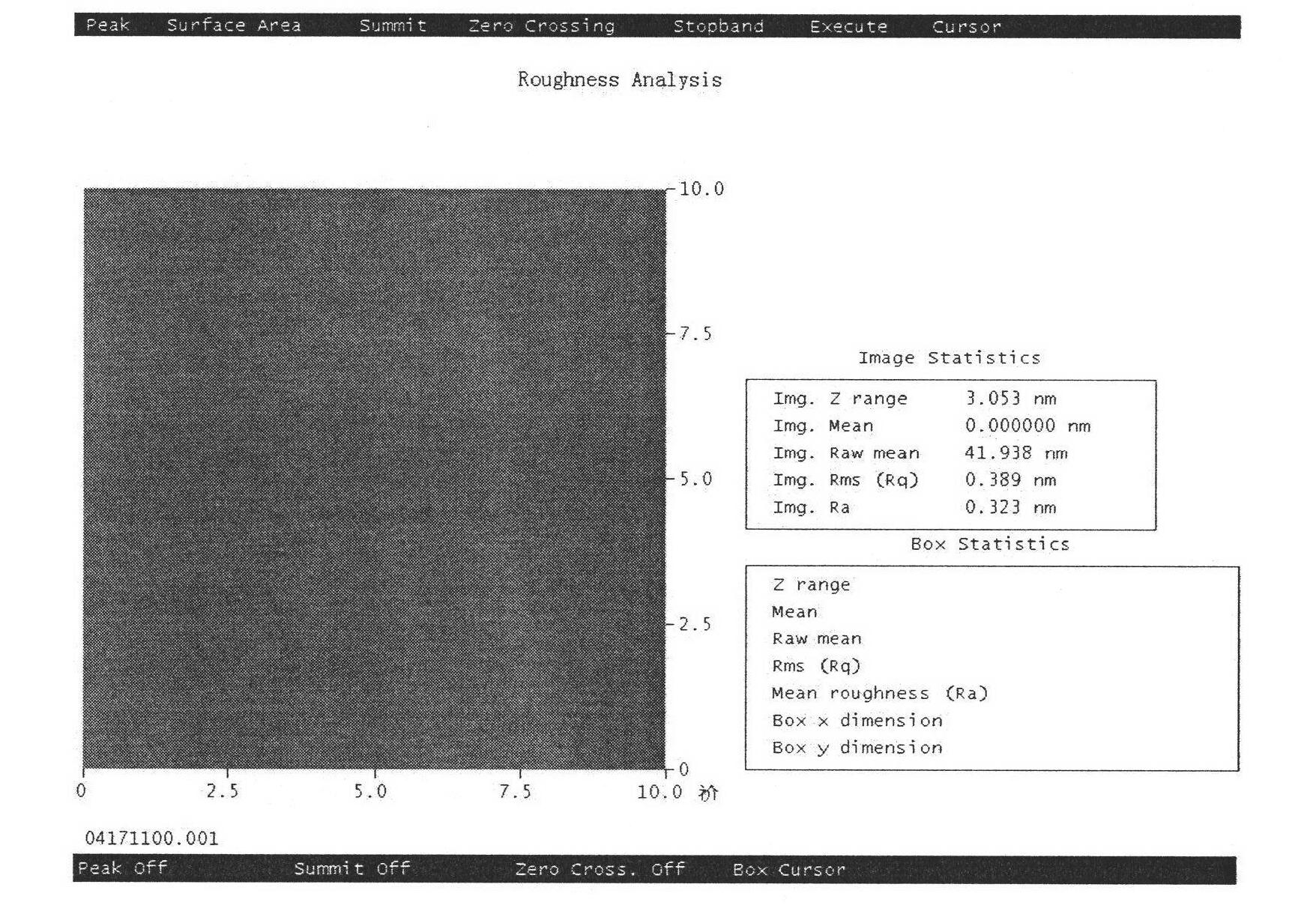
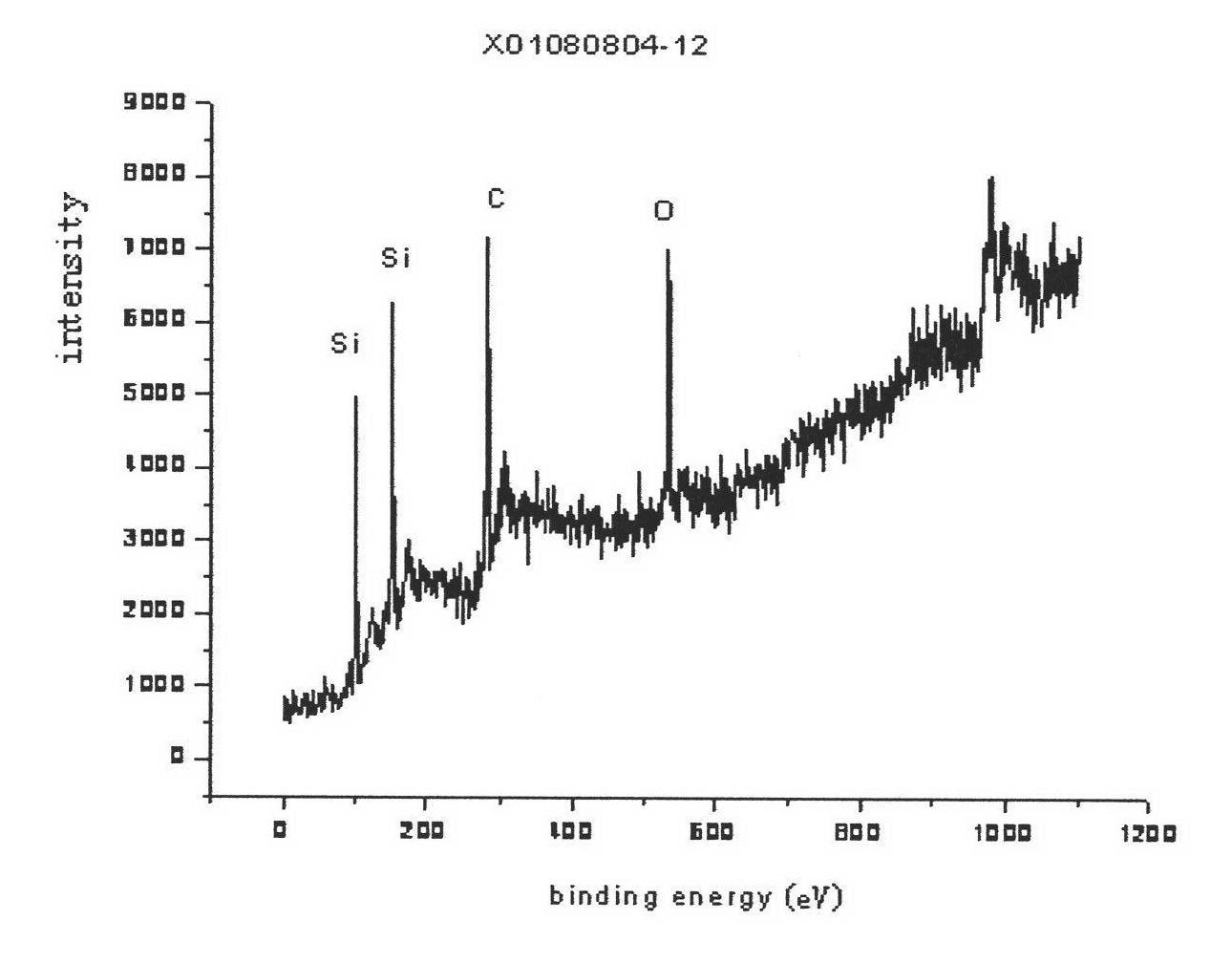
[0023] The silicon carbide wafer cleaned with acetone should achieve the following effect: no visible pollutants on the surface when observed under ...

Embodiment 2

[0028] Embodiment 2: Cleaning of the surface of a silicon carbide wafer with serious pollution.

[0029] The paraffin wax on the surface of the silicon carbide wafer was cleaned with acetone heated to 50°C. The cleaning process is the same as in Example 1. Place 3 cups of hot acetone solution to clean the silicon carbide wafers sequentially. After cleaning 6 wafers, replace the first cup of turbid acetone, and then use the same method for each 3 silicon carbide wafers. Replace with a cup of acetone.

[0030] There should be no visible contaminants on the surface of the silicon carbide wafer cleaned with acetone when observed under a strong light. Afterwards, the surface of the silicon carbide wafer was rinsed with deionized water and the silicon carbide wafer was ultrasonically cleaned in an ethanol solution. The specific cleaning method was the same as in Example 1.

[0031] Heat the silicon carbide wafer in 30% hydrogen peroxide solution at 70°C for 3 minutes, take out the...


PUM


Abstract

The invention provides a method for cleaning pollutants on the surface of a silicon carbide wafer. The cleaning process comprises two parts, namely an organic cleaning process and an inorganic cleaning process. The organic cleaning process comprises the step of removing waxiness adhered to the surface and other partial organic pollutants on the surface. The inorganic cleaning process comprises the step of removing residual organic pollutants and other strong-adsorptivity substances on the surface of the silicon carbide wafer through oxygenization and removing an oxide layer, and removing inorganic pollutants on the surface through acid-washing. By the cleaning process, pollutants and particles on the surface can be removed to the greatest extent and the instant utilization efficiency of the silicon carbide wafer is greatly improved.

Description

technical field [0001] The invention belongs to the field of wafer cleaning, and in particular relates to a cleaning method for cleaning pollutants on the surface of a silicon carbide wafer. Background technique [0002] Wide bandgap semiconductor materials represented by silicon carbide (SiC) and gallium nitride (GaN) are the third-generation semiconductors after silicon (Si) and gallium arsenide (GaAs). Compared with Si and GaAs traditional semiconductor materials, SiC has excellent properties such as high thermal conductivity, high breakdown field strength, high saturation electron drift rate and high bonding energy, and has great potential in high temperature, high frequency, high power and radiation resistant devices. Application prospects. In addition, due to the similar lattice constant and thermal expansion coefficient of SiC and GaN, it also has extremely broad application prospects in the field of optoelectronic devices. [0003] The surface of silicon carbide wa...

Claims


Application Information

Patent Timeline
IPC IPC(8): C23G1/02B08B3/08B08B3/12
Inventor 郭钰陈小龙王波张贺王锡铭彭同华郭晨丽鲍惠强李龙远郑红军
Owner BEIJING TIANKE HEDA SEMICON CO LTD
Why Eureka
Try Eureka