LED (Light Emitting Diode) surface patch type encapsulating structure based on silicon base plate and encapsulating method thereof

A packaging method and packaging structure technology, applied in the direction of electrical components, electrical solid devices, circuits, etc., can solve the problems of increased wiring difficulty, difficult multi-chip modules, poor temperature resistance, etc., to reduce process cost and process difficulty , Convenient connection and packaging at will, good heat dissipation effect

Inactive Publication Date: 2011-03-30
APT ELECTRONICS
View PDF6 Cites 59 Cited by
  • Summary
  • Abstract
  • Description
  • Claims
  • Application Information

AI Technical Summary

Problems solved by technology

However, the current LED surface mount structure has the following problems: since the packaging bracket 100 uses a metal bracket as the substrate, and then is sealed and cut by injecting plastic grooves or molding, its temperature resistance is not good. Good, heat dissipation is not ideal, miniaturization is not easy to manufacture
Because this structure needs to dig a large deep groove on the upper surface of the silicon wafer, it needs to etch the silicon wafer for a long time, the process is complicated and the cost is high; at the same time, because the groove is very deep, it is difficult to wire inside it, especially If flip chip is used, it is necessary to make metal bumps on the electrodes in the grooves, and the process is more difficult; moreover, because there are deep grooves on the upper surface of the silicon substrate, it is not easy to integrate the peripheral circuits of the LED on the silicon substrate (such as electrostatic protection circuits, drive circuits, etc.), its application prospects are also limited; in addition, due to the size of the groove, the number of chips placed in the groove is limited, and it is not easy to realize multi-chip modules

Method used


Image

  • LED (Light Emitting Diode) surface patch type encapsulating structure based on silicon base plate and encapsulating method thereof
  • LED (Light Emitting Diode) surface patch type encapsulating structure based on silicon base plate and encapsulating method thereof
  • LED (Light Emitting Diode) surface patch type encapsulating structure based on silicon base plate and encapsulating method thereof

Examples


Embodiment Construction

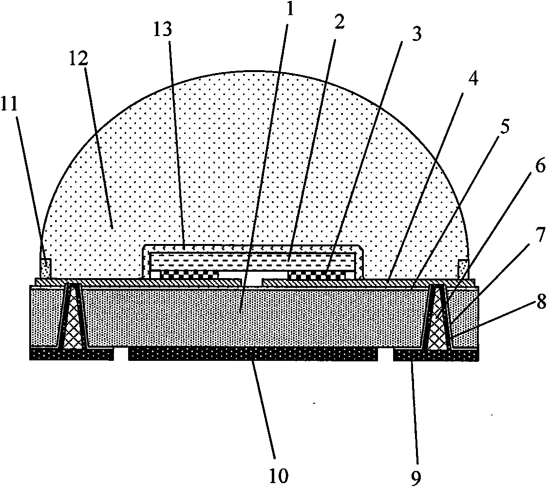
[0022] Please also see image 3 , Figure 4 and Figure 5 , which are respectively a schematic cross-sectional view, a top view and a bottom view of the silicon substrate-based LED packaging structure of the present invention. The LED packaging structure includes a silicon substrate 1 , an LED chip 2 and a lens 12 . Specifically, the upper surface of the silicon substrate 1 is a planar structure without grooves. An oxide layer 5 covers the upper surface of the silicon substrate 1 . Two metal electrode layers 4 respectively used to connect positive and negative electrodes are disposed on the upper surface of the oxide layer 5 and are insulated from each other. Metal bumps 3 are respectively provided on the upper surface of the metal electrode layer 4 . The LED chip 2 is flip-chip mounted on the silicon substrate 1 , and the positive and negative poles of the LED chip 2 are respectively connected to two metal bumps 3 , so as to be electrically connected to the metal electro...


PUM


Abstract

The invention relates to an LED (Light Emitting Diode) surface patch type encapsulating structure based on a silicon base plate, which comprises the silicon base plate, an LED chip, a circular ring convex wall and a lens, wherein the upper surface of the silicon base plate is a plane structure, an oxidation layer is covered on the upper surface of the silicon base plate, a metal electrode layer is arranged on the upper surface of the oxidation layer, the upper surface of the metal electrode layer is provided with metal convex points, a through hole penetrating through the silicon base plate is arranged below the metal electrode layer, an insulation layer covers the inner wall of the through hole and the partial lower surface of the silicon base plate, a metal connecting layer covers the surface of the insulation layer in the through hole, two electric conducting metal welding discs are respectively arranged at the lower surface of the silicon base plate and are insulated from the silicon base plate, a heat conducting metal welding disc is arranged at the lower surface of the silicon base plate, the LED chip is inversely arranged on the silicon base plate, and the LED chip and the metal electrode layer in the LED chip are isolated from the outside through the circular ring convex wall and the lens. The encapsulating structure has the advantages of good heat radiation effect and small size, also has high reliability because of no gold thread encapsulation, realizes the wafer level mass production encapsulation and hereby reduces the encapsulation cost.

Description

technical field [0001] The invention belongs to the field of manufacturing light-emitting devices, and relates to an LED packaging structure based on a silicon substrate and a packaging method thereof Background technique [0002] Light-emitting diode (LED) light sources have the advantages of high efficiency, long life, and no harmful substances such as Hg. With the rapid development of LED technology, the brightness and lifespan of LEDs have been greatly improved, making the application of LEDs more and more extensive. From outdoor lighting such as street lamps to indoor lighting such as decorative lamps, they are all used or replaced one after another. into LED as light source. [0003] LED surface mount type (SMD) packaging structure has become the main packaging form due to its advantages of convenient application and small size. see figure 1 , which is a commonly used LED surface mount structure in the prior art, including a package holder 100 and an LED chip 200 mo...

Claims


Application Information

Patent Timeline
Patent Type & Authority Applications(China)
IPC IPC(8): H01L33/48H01L33/58H01L33/62H01L33/64
CPCH01L33/64H01L33/486H01L2224/45144H01L33/62H01L2924/10253H01L2224/32225H01L2224/48227H01L2224/73265H01L33/54H01L2224/48091H01L2924/00014H01L2924/00
Inventor 肖国伟曾照明陈海英周玉刚侯宇
Owner APT ELECTRONICS
Why Eureka
Try Eureka