Laser micro/nano processing system and method

A micro-nano processing and laser technology, applied in laser welding equipment, metal processing equipment, nanotechnology, etc., can solve problems such as difficult material processing, and achieve the effect of expanding the scope of processing materials

Active Publication Date: 2011-04-06
TECHNICAL INST OF PHYSICS & CHEMISTRY - CHINESE ACAD OF SCI
View PDF6 Cites 60 Cited by
  • Summary
  • Abstract
  • Description
  • Claims
  • Application Information

AI Technical Summary

Problems solved by technology

However, the above techniques are limited to the processing of materials with properties that can be quenched by photoexcitation and excited state light, and it is difficult to process other types of materials

Method used


Image

  • Laser micro/nano processing system and method
  • Laser micro/nano processing system and method
  • Laser micro/nano processing system and method

Examples


example 1

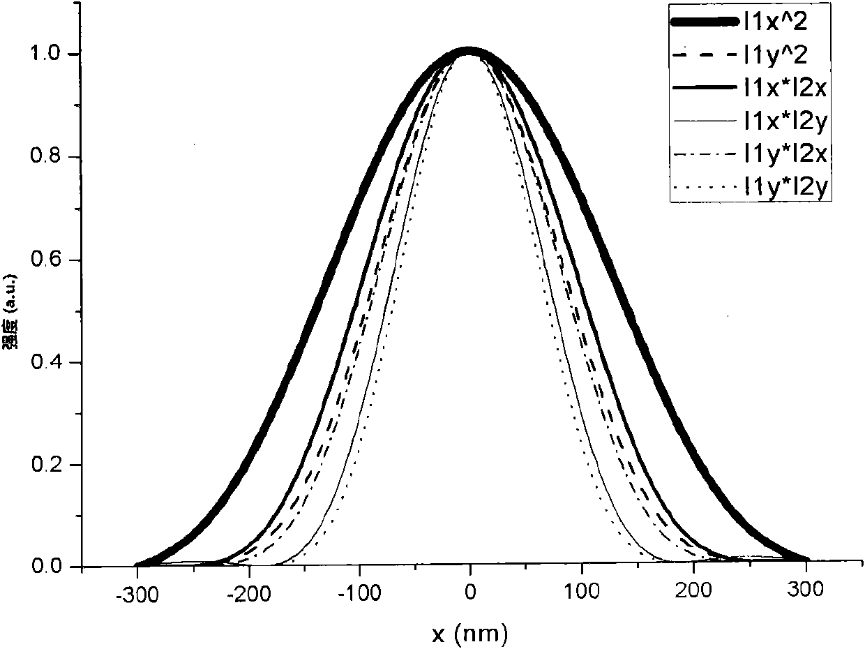
[0103] The specific implementation steps of preparing the line array structure in the photoresist with the trade name of SCR500 placed on the glass substrate will be described in detail below in conjunction with the laser micro-nano processing system according to the present invention.

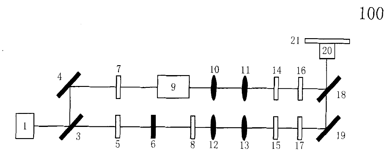
[0104] The laser micro-nano processing system 100 includes: a laser 1 , a half-mirror 3 , a frequency doubling crystal 5 , an optical delay component 9 , an optical focusing component and a moving platform 21 . The laser 1 is, for example, a titanium sapphire femtosecond pulsed laser with an output wavelength of 800 nm, a pulse width of 100 fs, a pulse repetition frequency of 82 MHz, a beam diameter of 1.8 mm, and a linearly polarized laser beam. On the output optical path of the Ti:Sapphire femtosecond pulsed laser 1 is placed a half-mirror 3 made of BK7 glass, for example, with a transmittance-reflection ratio of 7:3 to form transmitted light and reflected light. The frequency multiplier on ...

example 2

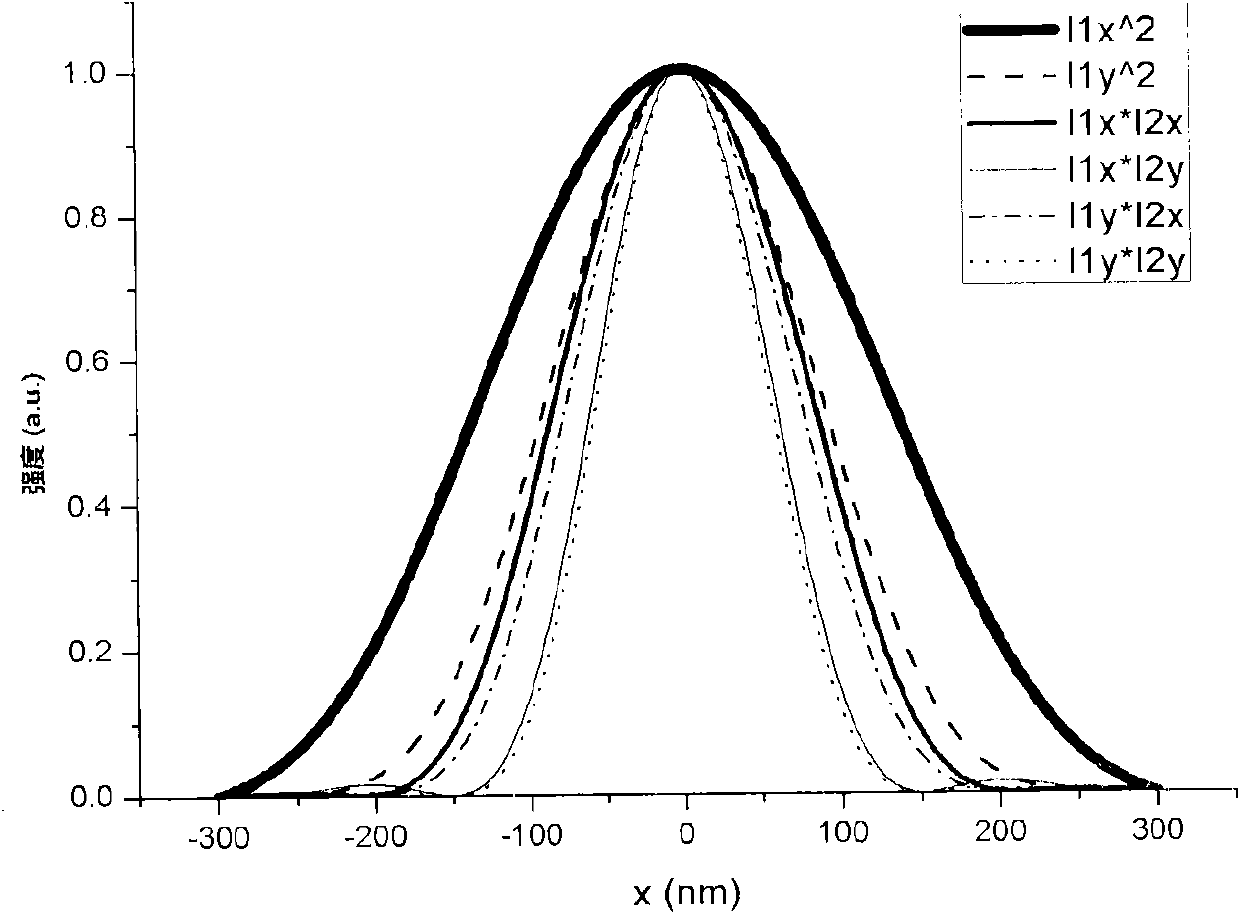
[0109] The following is attached image 3 The system of the present invention and the specific implementation steps of preparing the dangling wire structure in the photoresist with the trade name SCR500 placed on the glass substrate by the system are described in detail:

[0110] The system includes: the laser 1 is a titanium sapphire femtosecond pulse laser, the output wavelength of the laser 1 is 800nm, the pulse width is 100fs, the pulse repetition frequency is 82MHz, the beam diameter is 1.8mm, and the polarization state is linear polarization; firstly, turn on the titanium sapphire Femtosecond pulsed laser 1, a half mirror 3 made of BK7 glass is placed on the output optical path, and the transmission and reflection ratio is 7:3; an I-type BBO frequency-doubling crystal with a thickness of 1 mm is placed sequentially along the main axis on the transmitted optical path 5 and a piece of interference filter 6 filtering 800nm ​​wavelength to obtain pure beam diameter is 400nm wa...

example 3

[0112] The following combination image 3 The system of the present invention and the specific implementation steps for preparing a two-dimensional dot array structure in a photoresist with a trade name of SCR500 placed on a glass substrate using the system are described in detail:

[0113] The system includes: the laser 1 is a titanium sapphire femtosecond pulse laser, the output wavelength of the laser 1 is 800nm, the pulse width is 100fs, the pulse repetition frequency is 82MHz, the beam diameter is 1.8mm, and the polarization state is linear polarization; firstly, turn on the titanium sapphire Femtosecond pulsed laser 1, a half mirror 3 made of BK7 glass is placed on the output optical path, and the transmission and reflection ratio is 7:3; an I-type BBO frequency-doubling crystal with a thickness of 1 mm is placed sequentially along the main axis on the transmitted optical path 5 and a piece of interference filter 6 filtering 800nm ​​wavelength to obtain pure beam diamete...


PUM

PropertyMeasurementUnit
diameteraaaaaaaaaa

Abstract

The invention provides a laser micro/nano processing system and a laser micro/nano processing method. The system of the invention comprises a laser light source, an optical retardation component, an optical focusing component and a computer-controlled micro mobile station, wherein the laser light source is used for providing a first laser beam having a first wavelength and a second laser beam having a second wavelength, the pulse widths of the first laser beam and the second laser beam range from femtosecond to nanosecond and the first wavelength is different from the second wavelength; the optical retardation component is used for regulating the optical path of the first laser beam or the second laser beam so that the difference between the arrival times of the first laser beam and the second laser beam at a focus is not greater than the level life time for a photochromic material to be processed to be excited to an excited state; the optical focusing component is used for focusing the first laser beam and the second laser beam onto the same focus; and the computer-controlled micro mobile station is used for regulating a photochromic material on the computer-controlled micro mobile station to the focus.

Description

technical field [0001] The invention relates to a laser micro-nano processing method and a processing system, in particular to a laser micro-nano processing method and a system with precisely controllable processing resolution and processing accuracy. Background technique [0002] For more than half a century, lithography technology has been occupying the dominant position of micro-nano processing technology. When using laser technology for material processing, the processing resolution that can be achieved has been limited by the classical optical diffraction limit, and it is difficult to process at the nanometer scale. This problem is the core scientific problem that needs to be solved first in the development of nanophotonic processing technology. The focus of attention of scientists in this field. [0003] Femtosecond laser micro-nano processing is a new type of ultra-fine processing technology integrating ultra-fast laser technology, microscopic technology, ultra-high-...

Claims


Application Information

Patent Timeline
Patent Type & Authority Applications(China)
IPC IPC(8): B23K26/00B81C1/00B82B3/00B23K26/0622B23K26/362
Inventor 段宣明陈述董贤子赵震声
Owner TECHNICAL INST OF PHYSICS & CHEMISTRY - CHINESE ACAD OF SCI
Why Eureka
Try Eureka