

Clock domain crossing controller of digital control switch power supply and control method thereof
A switching power supply, cross-clock domain technology, applied in the field of electronics, can solve the problems of inability to realize real-time control of the system, inability to know the data cycle, not the latest data, etc., to save system power consumption, overcome data delay steady state, data Handle the effects of partial optimization
- Summary
- Abstract
- Description
- Claims
- Application Information
AI Technical Summary
Problems solved by technology
Method used
Image

Examples
Embodiment Construction
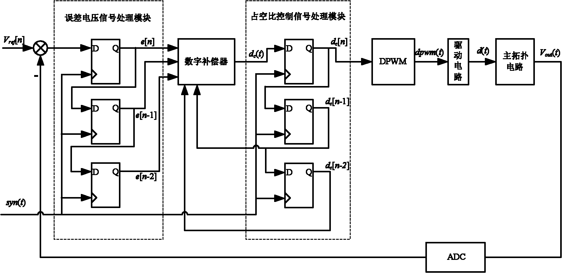
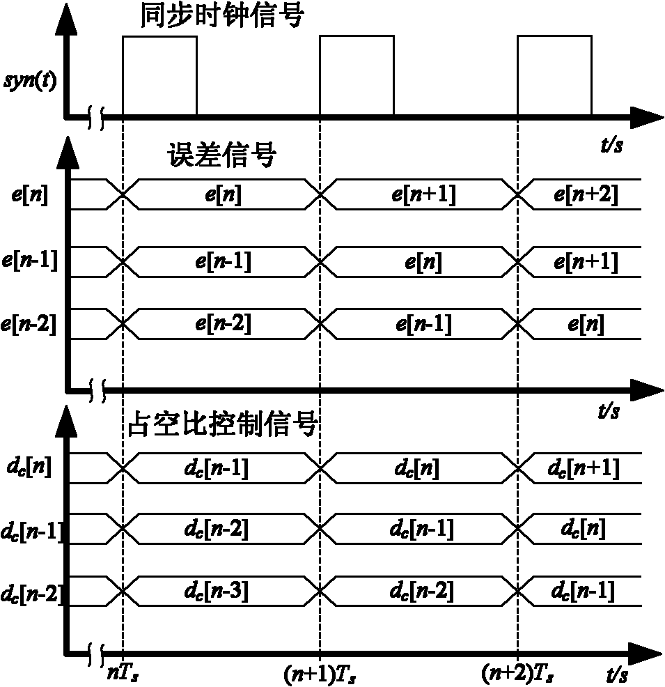
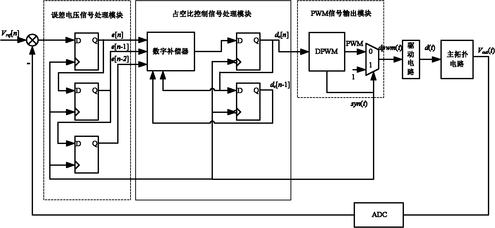
[0023] Such as image 3 and Figure 8 , the controller of the present invention includes a voltage divider network H sence , an analog-to-digital converter, an error voltage signal processing module, a digital compensator, a PWM signal output module, a drive circuit and a clock logic circuit. Switching power supply output data V out (t) After being divided by the voltage divider network, it is collected and quantified by the ADC to obtain V o [n], with a preset discrete reference voltage V ref The error voltage signal e[n] obtained by subtracting [n] is sent to the digital compensator for data processing, and then modulated by the digital pulse width modulation circuit DPWM to generate the voltage control signal of the switching power supply, which is controlled by the driving circuit after increasing the driving capacity The opening and closing of the power tube of the switching power supply. The controller adjusts the duty ratio once in each switching cycle of the switc...
PUM
 Abstract
Description
Claims
Application Information