Manufacturing method of SiGe heterojunction bipolar transistor

A technology of heterojunction bipolar and fabrication method, applied in semiconductor/solid-state device manufacturing, semiconductor device, electrical components and other directions, can solve the problems of complex process and complex process, and achieve the effect of simple process

Active Publication Date: 2011-05-11
SHANGHAI HUAHONG GRACE SEMICON MFG CORP
View PDF2 Cites 8 Cited by
  • Summary
  • Abstract
  • Description
  • Claims
  • Application Information

AI Technical Summary

Problems solved by technology

[0003] Existing device structures such as figure 1 As shown (US patent application US6,927,476): After the STI (Shallow Trench Isolation) process is completed, a series of processes are used to obtain a self-aligned device structure, and the process is complicated (after the STI process is completed and before the emitter is deposited, A total of more than 8 times of film growth process, secondary photolithography, secondary CMP (chemical mechanical polishing), 6 times of film etching); another structure such as figure 2 As shown (US patent application US7,037,798), the construction of the SiGe HBT is also started after the completion of the STI process. From the completion of the STI process to the deposition of the emitter, a total of more than 7 film growth processes have been added. engraving, 6 times of film etching), there is also the problem of complex process

Method used


Image

  • Manufacturing method of SiGe heterojunction bipolar transistor
  • Manufacturing method of SiGe heterojunction bipolar transistor
  • Manufacturing method of SiGe heterojunction bipolar transistor

Examples


Embodiment Construction

[0033] The present invention will be described in further detail below in conjunction with the accompanying drawings and embodiments.

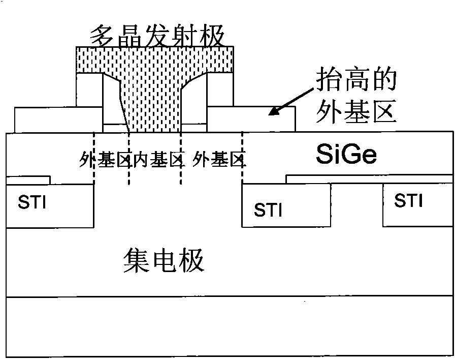
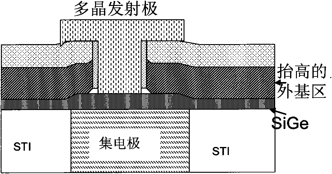
[0034] The invention discloses a manufacturing method of a germanium-silicon heterojunction bipolar transistor (HBT, heterojunction bipolar transistor) with an elevated extrinsic base region and self-alignment between the extrinsic base region and the emitter, which combines the shallow trench isolation process module The materials and processes used in the above are to form highly doped P-type polysilicon that increases the outer base region, and then use the selective epitaxy process to form the inner base region of the germanium-silicon heterojunction bipolar transistor region, and finally use the dielectric film as the emitter The isolation layer between the electrode and the extrinsic base region, and the emitter electrode is deposited.

[0035] The device main technology of a heterojunction bipolar transistor (NPN) is taken as an example...


PUM

PropertyMeasurementUnit
thicknessaaaaaaaaaa
thicknessaaaaaaaaaa
thicknessaaaaaaaaaa

Abstract

The invention discloses a manufacturing method of a SiGe heterojunction bipolar transistor. The method comprises the following steps of: forming high P-type doped polycrystalline silicon which raises an outer base region in combination with materials and a process used in a shallow slot isolation process module; forming an inner base region of a germanium-silicon heterojunction bipolar transistor region by using a selective epitaxial process; and depositing an emitter by taking a medium film as an isolation layer between the emitter and the outer base region so as to form a raised outer base region, wherein a self-aligned germanium-silicon heterojunction bipolar transistor is arranged between the outer base region and the emitter. Process steps are reduced, manufacturing time is shortened and manufacturing cost is lowered.

Description

technical field [0001] The invention belongs to the field of semiconductor integrated circuit manufacturing, in particular to a method for manufacturing a SiGe (silicon germanium) heterojunction bipolar transistor. Background technique [0002] Since SiGe HBT (SiGe Heterojunction Bipolar Transistor) has high-speed and low-noise requirements, it has more and more applications in the radio frequency field. While people in the industry are constantly working hard to improve its operating frequency (increase the speed of use), it has good competitiveness in cost, that is, it strives to make its performance reach GaAs (gallium arsenide) devices with lower cost (using CMOS process And have good compatibility with CMOS). In order to increase the speed, it has become a consensus to raise the position of the outer base area to reduce the capacitance of the base-collector area, and to use the self-alignment of the outer base area and the emitter to obtain a low base area resistance. ...

Claims


Application Information

Patent Timeline
Patent Type & Authority Applications(China)
IPC IPC(8): H01L21/331H01L21/20H01L29/737H01L29/10
Inventor 肖胜安
Owner SHANGHAI HUAHONG GRACE SEMICON MFG CORP
Why Eureka
Try Eureka