LDMOS (laterally diffused metal oxide semiconductor) and manufacturing method thereof

A doping type and heavy doping technology, which is applied in semiconductor/solid-state device manufacturing, electrical components, circuits, etc., can solve the problems of LDMOS device threshold voltage drift, transconductance reduction, and driving ability decline

Active Publication Date: 2011-05-11
SHANGHAI HUAHONG GRACE SEMICON MFG CORP
View PDF0 Cites 13 Cited by
  • Summary
  • Abstract
  • Description
  • Claims
  • Application Information

AI Technical Summary

Problems solved by technology

However, when the drain terminal voltage of the above-mentioned LDMOS device is high, the carriers (electrons and holes) in the channel region are still relatively easy to obtain high kinetic energy

Method used


Image

  • LDMOS (laterally diffused metal oxide semiconductor) and manufacturing method thereof
  • LDMOS (laterally diffused metal oxide semiconductor) and manufacturing method thereof
  • LDMOS (laterally diffused metal oxide semiconductor) and manufacturing method thereof

Examples


Embodiment Construction

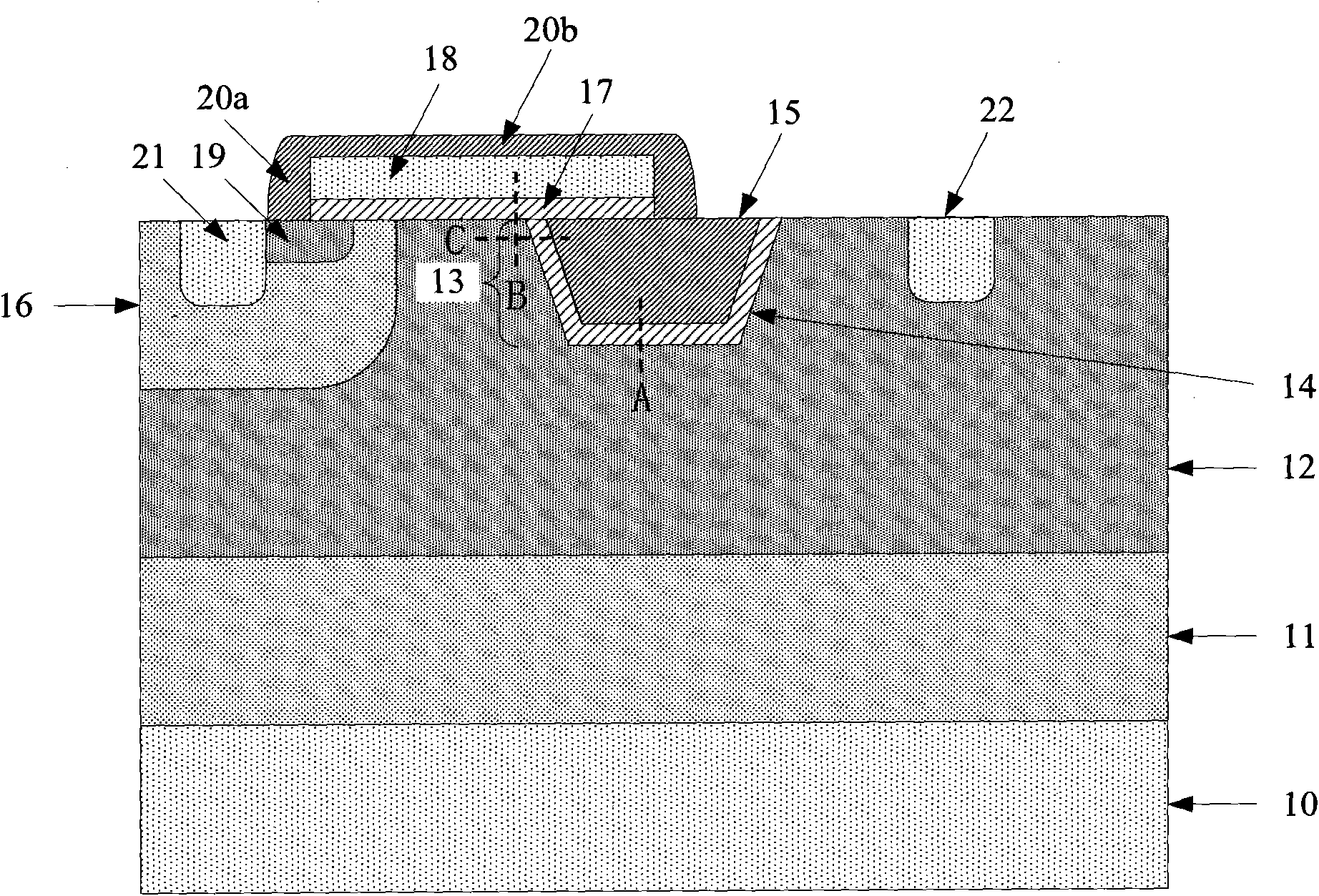
[0041] The structure of the LDMOS device of the present invention will be described below by taking an n-type LDMOS as an example.

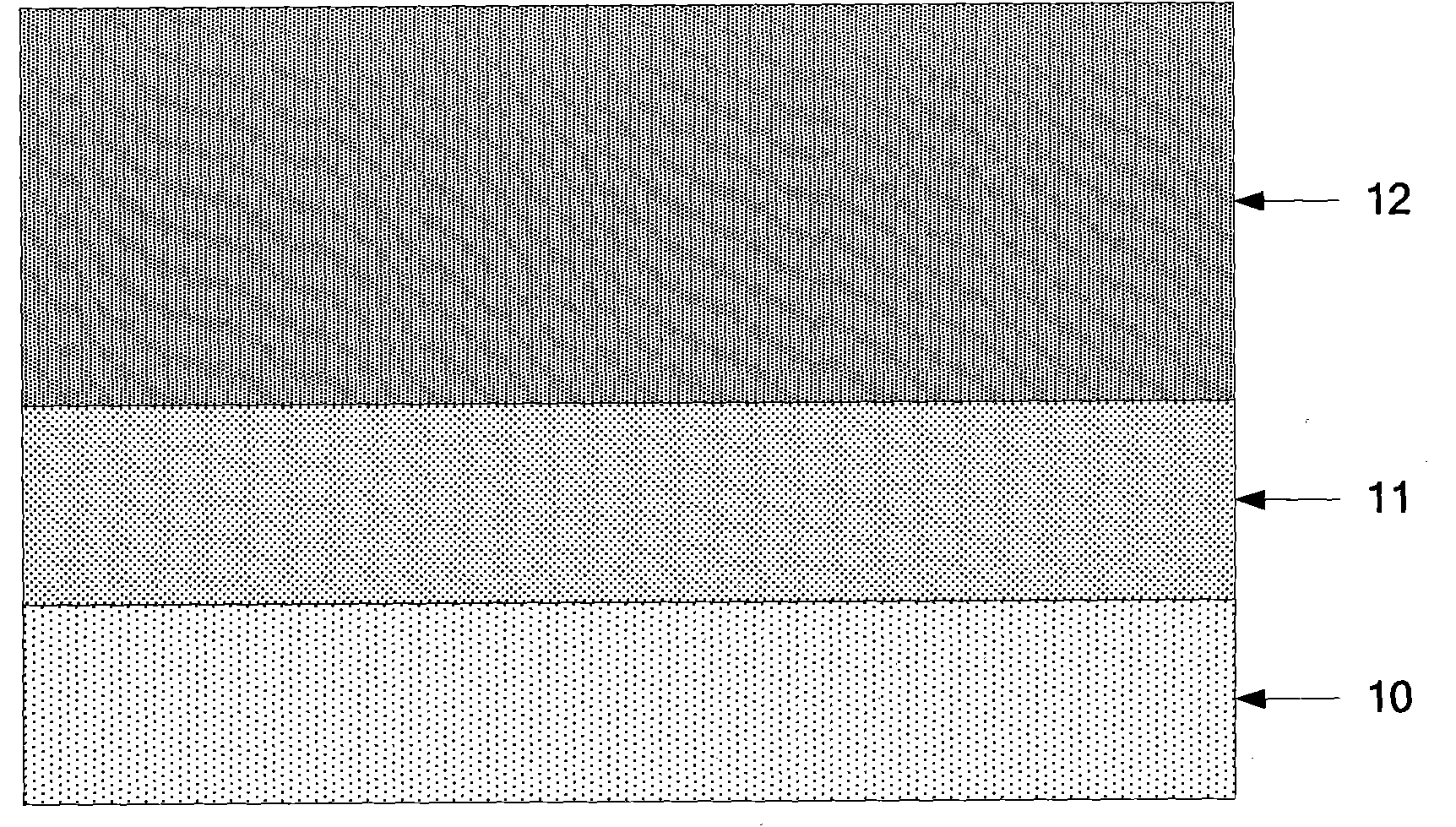
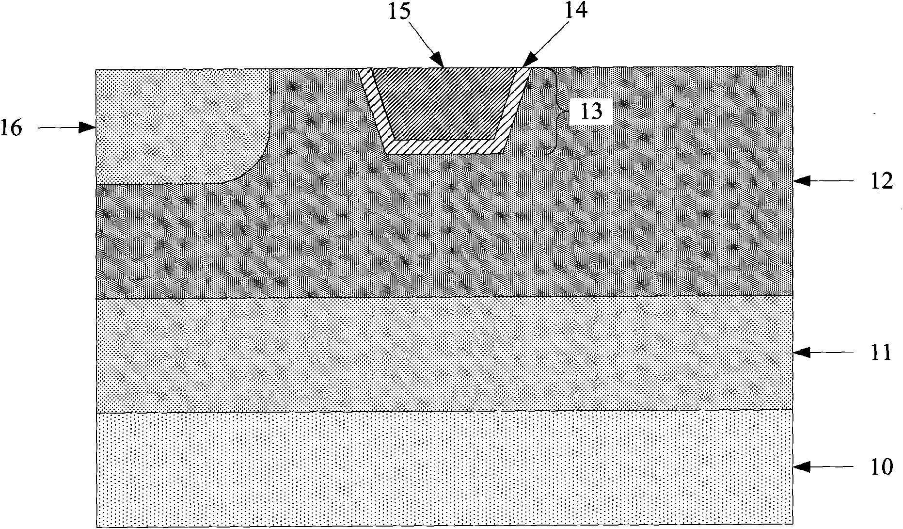
[0042] see image 3 , The n-type LDMOS of the present invention respectively includes a p-type substrate 10, a p-type epitaxial layer 11 and an n-well 12 from bottom to top. The thickness of the n well 12 is usually 4-5 μm, and it is sometimes called "deep n well". The n well 12 has a trench 13, a p well 16, and an n-type heavily doped drain region 22, and the p well 16 and the n-type heavily doped drain region 22 are respectively on both sides of the trench 13 and are not in phase with the trench 13. coincident (that is, they are all at a certain distance from the groove 13). A pad oxide layer 14 is formed on the sidewall and bottom of the trench 13 , and the trench 13 is filled with a shallow trench isolation structure 15 (usually a dielectric material such as silicon oxide, silicon nitride, silicon oxynitride, etc.). There is an n-type ligh...


PUM


Abstract

The invention discloses a LDMOS. Based on the traditional LDMOS (laterally diffused metal oxide semiconductor) structure, a light dope area (30) is arranged on the side wall and the bottom close to a groove (13) in a well (12). The doping types of the light dope area (30) and the well (12) are the same and the doping density of the light dope area (30) is lower. The invention also discloses a manufacturing method of an LDMOS. The shifting area of the traditional LDMOS is the well (12) but the shifting area of the LDMOS provided by the invention is the well (12) and the light dope area (30), so that the electric field along vertical and horizontal directions of the groove in the LDMOS provided by the invention is conveniently reduced, therefore reducing the electron collision strength in the shifting area, restraining the hot carrier injection effect, and increasing the safety working area and reliability of the LDMOS device.

Description

technical field [0001] The invention relates to an electronic device and a manufacturing method thereof, in particular to an LDMOS and a manufacturing method thereof. Background technique [0002] LDMOS (laterally diffused MOSFET, laterally diffused MOS transistor) is widely used in power amplifiers in the radio frequency and microwave fields. [0003] see figure 1 , which is a schematic diagram of the existing structure of n-type LDMOS fabricated by BCD (bipolar, CMOS and DMOS) process. On the p-type silicon substrate 10 are a p-type epitaxial layer 11 and an n-well 12 respectively. The thickness of the n well 12 is, for example, 4 to 5 μm. The n-well 12 has a trench 13 , a p-well 16 and an n-type heavily doped drain region 22 . The p-well 16 and the n-type heavily doped drain region 22 are respectively on both sides of the trench 13 and neither overlaps with the trench 13 (that is, both are separated from the trench 13 by a certain distance). The sidewall and the bott...

Claims


Application Information

Patent Timeline
IPC IPC(8): H01L29/78H01L29/36H01L21/336H01L21/265
CPCH01L29/0878H01L29/7816H01L29/0653H01L29/66689H01L29/1083
Inventor 张帅戚丽娜吕赵鸿
Owner SHANGHAI HUAHONG GRACE SEMICON MFG CORP
Why Eureka
Try Eureka