Shallow-slot metal oxide semiconductor diode

An oxide semiconductor and diode technology, applied in semiconductor devices, electrical components, circuits, etc., can solve the problems of low reverse breakdown voltage, limited application range, low reverse withstand voltage value, etc., to improve the breakdown voltage, The effect of low leakage current and good forward voltage drop

Inactive Publication Date: 2011-05-18
深圳市芯威科技有限公司
View PDF2 Cites 13 Cited by
  • Summary
  • Abstract
  • Description
  • Claims
  • Application Information

AI Technical Summary

Problems solved by technology

Since the reverse barrier of Schottky diodes is relatively thin, and it is easy to break down on its surface, the reverse breakdown voltage is relatively low, and the reverse withstand voltage value is low, most of which are not higher than 60V, and the highest is only about 100V , which limits its scope of application

Method used


Image

  • Shallow-slot metal oxide semiconductor diode
  • Shallow-slot metal oxide semiconductor diode
  • Shallow-slot metal oxide semiconductor diode

Examples


Embodiment Construction

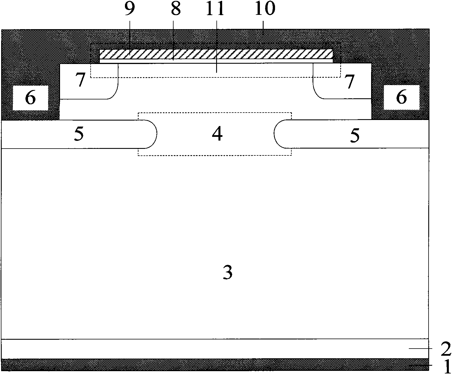
[0021] The present invention will be described in further detail below in conjunction with the accompanying drawings and embodiments. Such as figure 1 As shown, the shallow groove metal oxide semiconductor diode of the present invention is provided with a metallized cathode 1, an N-type heavily doped single crystal silicon substrate region 2, an N - Epitaxial layer 3 , two deep P body regions 5 , shallow groove 6 , N-type heavily doped region 7 , silicon dioxide gate oxide layer 8 , polysilicon gate electrode 9 and metalized anode 10 .

[0022] The physical structure of the shallow groove metal oxide semiconductor diode is metallized cathode 1, N-type heavily doped single crystal silicon substrate region 2, N - Epitaxial layer 3, two deep P body regions 5 on both sides, shallow trench 6 on deep P body region 5, N-type heavily doped region 7 inside shallow trench 6, silicon dioxide gate oxide layer 8, polysilicon Gate electrode 9, metalized anode 10.

[0023] The metallized ...


PUM


Abstract

The invention discloses a shallow-slot metal oxide semiconductor diode for solving reducing the forward conduction voltage drop of the diode, increasing reverse breakdown voltage and reducing leakage current. The shallow-slot metal oxide semiconductor diode provided by the invention comprises a metallized cathode, an N-type heavily-doped monocrystalline silicon substrate region, an N-epitaxial layer, two deep P regions located on two sides, shallow slots located on the deep P regions, N-type heavily-doped regions on the inner sides of the shallow slots, a silicon dioxide gate oxide layer, a polycrystalline silicon gate electrode and a metallized anode, which are arranged in sequence from the bottom layer to the top. Compared with the prior art, by adopting the electron accumulation layer structure and the junction field-effect tube structure, the invention can obtain extremely low conduction voltage drop, greatly improve the breakdown voltage, and reduce the leakage current. Under reverse voltage, the thin gate oxide layer accelerates the pinch-off of a conducting channel on a semiconductor surface, and the compromise between forward conduction voltage drop and reverse recovery time is better realized, and therefore, the shallow-slot metal oxide semiconductor diode provided by the invention has better compromise between forward conduction voltage drop and reverse recovery time.

Description

technical field [0001] The invention relates to a semiconductor device, in particular to a metal oxide semiconductor diode. Background technique [0002] In electronic circuits, diodes are one of the most commonly used basic electronic components; in power electronic circuits, diodes go hand in hand with switching devices and are indispensable. Traditional rectifier diodes mainly include PN junction diodes and Schottky diodes. Among them, the PN junction diode has a large forward conduction voltage drop and a long reverse recovery time, but the PN junction diode has better stability and can work at high voltage; Schottky diode has an absolute advantage at low voltage: its forward conduction The on-voltage drop is small and the reverse recovery time is short, but the leakage current of the Schottky diode is relatively high and unstable when it reverses. In order to improve the performance of diodes, junction barrier control rectifier JBS (JBS: Junction Barrier Controlled Sc...

Claims


Application Information

Patent Timeline
Patent Type & Authority Applications(China)
IPC IPC(8): H01L29/861H01L29/06H01L29/40
Inventor 李泽宏唐文雄
Owner 深圳市芯威科技有限公司
Why Eureka
Try Eureka