Double-sided printed circuit board (PCB) with elements and mutual conductance method thereof

A double-sided, component technology, applied in the field of interconnection and conduction, can solve the problems of consuming large phenolic tree branch cover boards and wood fiber bottom boards, cannot produce boards larger than 762mm, and cannot meet the needs of technological development, etc., to achieve the quality of circuit boards Reliable, reduce chemical wastewater discharge, reduce the effect of chemical treatment process

Active Publication Date: 2011-05-18
王定锋
View PDF0 Cites 4 Cited by
  • Summary
  • Abstract
  • Description
  • Claims
  • Application Information

AI Technical Summary

Problems solved by technology

This method causes serious pollution to the environment due to the need for electroplating and electroless plating
[0003] However, the traditional carbon oil filling hole or silver paste filling hole is usually used to form conduction on both sides of the double-sided printed circuit without copper plating, which has its obvious disadvantages. The cost of carbon oil filling is low, but due to carbon Oil has high resistance and poor conductivity; while silver paste has good conductivity, but the price of silver paste is very expensive and not suitable for mass production.
[0004] At the same time, the mechanical drilling machine and laser drilling machine in the traditional production process are expensive, the drilling speed is slow, and the production efficiency is low
And because the mechanical drilling machine is a pl...

Method used


Image

  • Double-sided printed circuit board (PCB) with elements and mutual conductance method thereof
  • Double-sided printed circuit board (PCB) with elements and mutual conductance method thereof
  • Double-sided printed circuit board (PCB) with elements and mutual conductance method thereof

Examples


Embodiment Construction

[0059] The present invention will be described in more detail below by taking a double-sided flexible printed circuit board as a specific embodiment. It should be understood by those skilled in the art that these embodiments are only some specific examples of the present invention, without any limitation on the present invention and its protection scope. For example, although the embodiments are described below in conjunction with copper foil, the material of the wiring layer not only includes pure copper, but also other copper alloys or other metals or alloys.

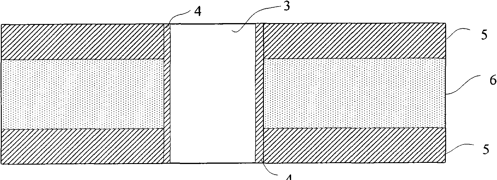
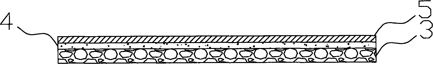
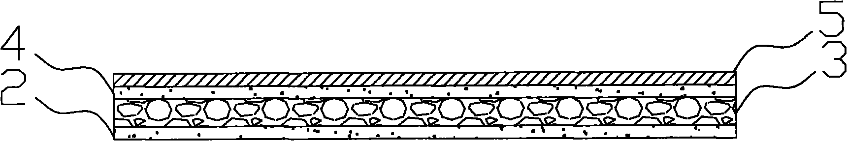
[0060] 1. Production of substrate

[0061] will be like figure 2 The shown rolled copper foil 5 thickness is preferably 12.5-35 microns, the thickness of the adhesive 4 is preferably 12.5-25 microns, and the thickness of the insulating film 3 is preferably 12.5-25 microns. On the film laminating machine, at 120-150 ° C, the pressure is 5-8kg / cm2 and the speed is 0.8-1.0m / min, and the thermosetting adhesive film 2 is...


PUM


Abstract

The invention discloses a double-sided printed circuit board (PCB) with elements and a mutual conductance method thereof, and provides a method for realizing mutual conductance by elements used in a double-sided PCB. The method comprises the following steps: providing the double-sided PCB with holes, wherein, the PCB comprises a top circuit layer, a bottom circuit layer and an insulating film layer bonded between the top circuit layer and the bottom circuit layer, and the holes pass through the top circuit layer and the insulating film layer besides the bottom circuit layer; optionally forming the bottom circuit layer at the holes to be aligned with or approximately aligned with the top circuit layer; and welding one part of the elements on the top circuit layer, and welding the other part of the elements on the bottom circuit layer at the holes so as to realize mutual conductance of the two circuit layers. The mutual conductance method is simple and low in cost; and double-sided circuits are conducted without eletcroless copper plating during the manufacturing process, thus being very environmental-friendly. The invention further discloses the PCB with the elements manufactured by the method.

Description

technical field [0001] The present invention relates to the field of printed circuit boards, in particular to a new method of interconnection and conduction such as double-sided flexible circuit boards (FPC) or rigid circuit boards, for example, directly soldering the component pins on the other side of the circuit through SMT reflow to make the double-sided The circuit on both sides of the circuit board is conductive. The invention also discloses the non-chemical method of forming the via hole without drilling and copper plating, and this method is more convenient for making continuous rolls of double-sided light strip circuit boards. Background technique [0002] In the traditional double-sided circuit board manufacturing process, mechanical drilling or laser drilling is generally used to drill circuit via holes on the copper clad laminate, and then the chemical copper plating process is used to make the double-sided flexible printed circuit board The inner wall of the th...

Claims


Application Information

Patent Timeline
IPC IPC(8): H05K3/32H05K3/34H05K1/18F21S4/00F21V23/00F21Y101/02
CPCH05K1/112H05K2201/094H05K2201/10106H05K3/4084H05K3/3442H05K2201/10636H05K2201/0394H01L2224/16225Y02P70/50
Inventor 王定锋张平
Owner 王定锋
Why Eureka
Try Eureka