Device for testing metallic film failure behaviors under the coupling of force, heat, power and magnetism multi-field

A metal thin film, magnetic coupling technology, applied in measurement devices, single semiconductor device testing, instruments, etc., can solve the problems of open-circuit failure, system catastrophic, errors, etc., and achieve the effect of reducing failure rate, easy to promote, and practical promotion.

Inactive Publication Date: 2011-06-01
XI AN JIAOTONG UNIV
View PDF8 Cites 20 Cited by
  • Summary
  • Abstract
  • Description
  • Claims
  • Application Information

AI Technical Summary

Problems solved by technology

at 10 10 A/m 2 Under the working current density of the order of magnitude, the internal stress and its redistribution caused by the resistance heating effect make the polycrystalline thin film aluminum wire experience the appearance of protrusions and depressions along the grain boundaries and gr

Method used


Image

  • Device for testing metallic film failure behaviors under the coupling of force, heat, power and magnetism multi-field
  • Device for testing metallic film failure behaviors under the coupling of force, heat, power and magnetism multi-field
  • Device for testing metallic film failure behaviors under the coupling of force, heat, power and magnetism multi-field

Examples


Embodiment 1

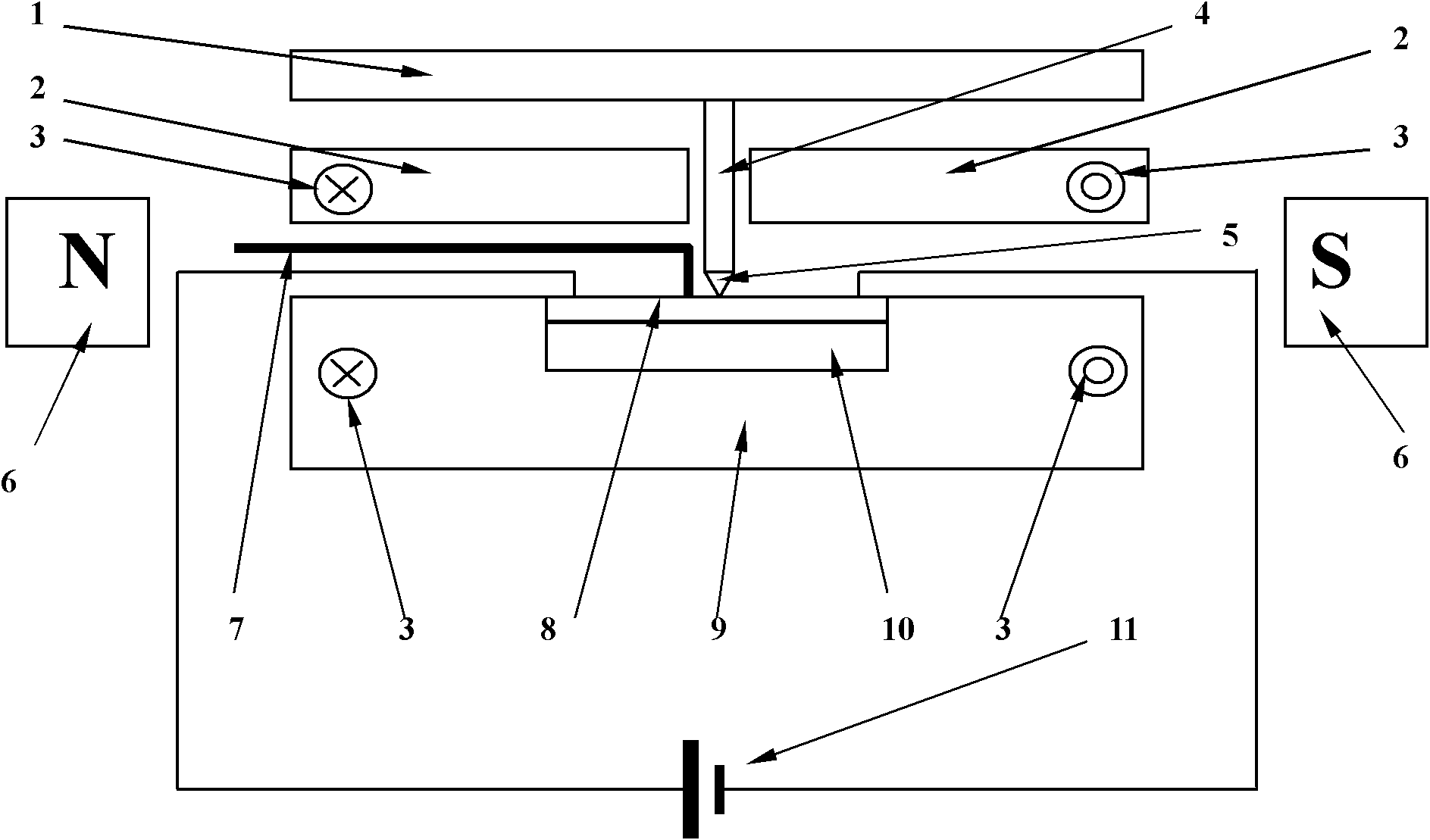
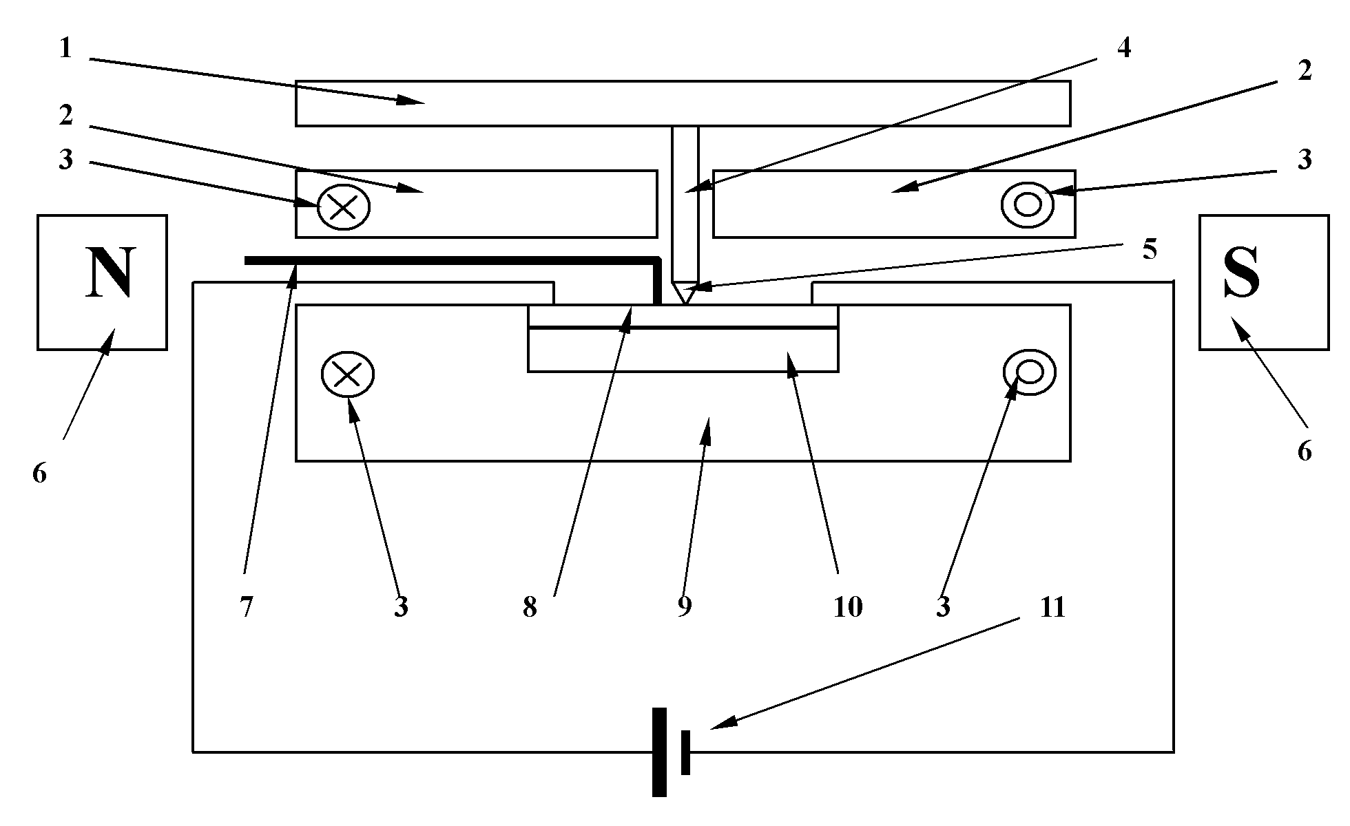
[0024] A metal Cu film with a line width of 2 microns was deposited on single crystal Si by photolithography and magnetron sputtering, and a TaN barrier layer was plated between the Cu film and Si to prevent Cu from diffusing to Si. Place the Cu film at 8 places in the device, turn on the heating platform 10, and control the constant direct current with a current intensity of 0.5A through a micro-nano digital ammeter. The magnetic pole 6 is placed on both sides of the heat insulation platform 9 perpendicular to the metal film, and applied in parallel. While applying a steady magnetic field, the film is heated to 100°C, protected by an argon atmosphere (to avoid oxidation) and cooled by circulating water. The magnetic induction intensity selected for the test is 0.5T. Using the fixed maximum load method, take P max = 100 μN, the load-displacement curve was obtained by a nanoindenter, and repeated 20 times. The load-displacement curve has good repeatability, indicating that th...

Embodiment 2

[0026] A metal Cu film with a line width of 2 microns was deposited on single crystal Si by photolithography and magnetron sputtering, and a TaN barrier layer was plated between the Cu film and Si to prevent Cu from diffusing to Si. Place the Cu film at 8 places in the device, turn on the heating platform 10, and control the constant direct current with a current intensity of 0.3A through a micro-nano digital ammeter. The magnetic pole 6 is placed on both sides of the heat insulation platform 9 perpendicular to the metal film, and applied in parallel. While applying a steady magnetic field, the film is heated to 100°C, protected by an argon atmosphere (to avoid oxidation) and cooled by circulating water. The magnetic induction intensity selected for the test is 0.3T. Using the fixed maximum load method, take P max = 150 μN, the load-displacement curve was obtained by a nanoindenter, and repeated 20 times. The load-displacement curves are very repeatable, indicating that the ...


PUM

PropertyMeasurementUnit
Hardness valueaaaaaaaaaa

Abstract

The invention discloses a device for testing metallic film failure behaviors under the coupling of force, heat, power and magnetism multi-field, which is characterized in that a warm table of embedded resistance wires is arranged above a heat insulation table; the warm table is connected with a power supply; the two ends of the heat insulation table are filled with convection circulating cooling water; a tested metallic film is arranged on the warm table; a thermocouple is arranged on a sample surface; a nanoindentation gearing is connected with a transmission rod; the two sides of the transmission rod between the nanoindentation gearing and the tested metallic film are respectively provided with a thermal baffle; the two sides of each thermal baffle are provided with circulating cooling water; and magnetic poles are arranged at the two sides of the heat insulation table. The device provided by the invention is used to improve prediction and evaluation level for failure behaviors of an electric thin-film material of an integrated circuit, is simple in operation, can really test and reflect failure performances of micro-components under the condition of actual services.

Description

technical field [0001] The present invention relates to the failure mechanism testing of metal thin films used in micro-electromechanical systems (MEMS) and nano-electromechanical systems (NEMS) under nearly actual service conditions, in particular to a device for testing the failure behavior of metal thin films under force / thermal / electric / magnetic multi-field coupling . Background technique [0002] An important reason for the failure of integrated circuits is that the coupling effects of mechanics, heat and electricity have not been dealt with. To study the thermal mismatch, creep, deformation, damage, mesoscopic fracture and solder joint damage of multi-layer microelectronic components and packages related to multi-field coupling, as well as the electromigration of inner wires, etc., for high-reliability devices and packages Failure prevention is very necessary. In the cross-century development of China's microelectronics industry, a new field of microelectromechanical...

Claims


Application Information

Patent Timeline
IPC IPC(8): G01R31/26G01N3/00
Inventor 王飞黄平卢天健徐可为
Owner XI AN JIAOTONG UNIV
Why Eureka
Try Eureka