

High-reflectivity light-emitting diode chip with vertical structure and preparation method thereof
A technology of light emitting diodes and high reflectivity, applied in the field of chips, can solve the problems of unsatisfactory improvement of light extraction efficiency, and the light extraction efficiency of devices has not been significantly improved, and achieves the effects of increasing light reflection efficiency, reducing loss and high lumen efficiency.
- Summary
- Abstract
- Description
- Claims
- Application Information
AI Technical Summary
Problems solved by technology
Method used
Image

Examples
Embodiment Construction
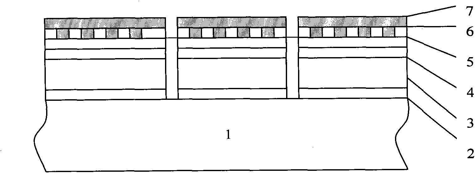
[0012] The preparation method of the light-emitting diode chip with the vertical structure in the embodiment of the present invention is as follows:
[0013] 1. Epitaxial growth on the substrate 1, sequentially growing buffer layer 2, N-type layer 3, multi-quantum well layer 4, and P-type layer 5;
[0014] 2. Through photolithography, dry etching until the sapphire substrate (etching depth is about 7um);
[0015] 3. Deposit a passivation layer (silicon dioxide) to protect the etched sidewall;
[0016] 4. Evaporation of DBR reflective layer 6
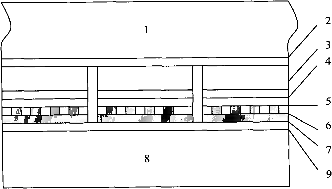
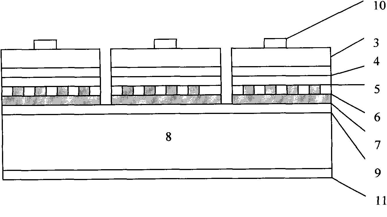
[0017] 5. DBR layer photolithography, corrosion (form 30 small holes with a diameter of 3-5um), vapor deposition of ohmic contact layer 7 (Ni / Ag / Ti / Au);
[0018] 6. Vapor-deposit a binding metal layer 9 (TiAlTiAu) on the heat dissipation substrate 8;
[0019] 7. Binding substrate and LED wafer;
[0020] 8. Combining chemical mechanical polishing and dry etching to remove the sapphire substrate and expose the N-type layer;
[002...
PUM
 Abstract
Description
Claims
Application Information