Trench metal oxide semiconductor field effect transistor and manufacturing method thereof

A technology of oxide semiconductors and field effect transistors, which is applied in the field of trench metal oxide semiconductor field effect transistors and its manufacturing, can solve the problems of high production costs, achieve the goal of reducing area, reducing resistance, and weakening parasitic transistor effects Effect

Inactive Publication Date: 2011-06-29
CHENGDU PROMISING CHIP ELECTRONICS
View PDF4 Cites 10 Cited by
  • Summary
  • Abstract
  • Description
  • Claims
  • Application Information

AI Technical Summary

Problems solved by technology

[0003] Due to its specific structure, the traditional trench metal oxide semiconductor field effect transistor (Trench MOSFET) requires seven layers of masks in the manufacturing process, and the production cost high

Method used


Image

  • Trench metal oxide semiconductor field effect transistor and manufacturing method thereof
  • Trench metal oxide semiconductor field effect transistor and manufacturing method thereof
  • Trench metal oxide semiconductor field effect transistor and manufacturing method thereof

Examples


Embodiment

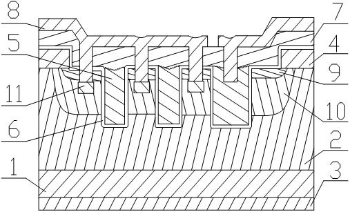
[0034] Such as figure 1 As shown, the trench metal oxide semiconductor field effect transistor includes an N+ substrate layer 1, the upper and lower end surfaces of the N+ substrate layer 1 are respectively provided with an N- epitaxial layer 2 and a back metal layer 3, and the back metal layer 3 forms a drain electrode. An annular field oxide layer 4 is arranged on the upper end of the N-epitaxial layer 2, and the N-epitaxial layer 2 is provided with a groove, and the groove is filled with a doped polysilicon layer 5, and the doped substance is preferably phosphorus or arsenic, Concentration order of magnitude 10 20 cm -3 , As preferably, the polysilicon layer 5 is 4800 Angstroms higher than the level of the trench opening. Between the N-epitaxial layer 2 and the polysilicon layer 5, the upper end surface of the N-epitaxial layer 2, and the upper end surface and the inner sidewall of the field oxide layer 4 are all provided with a gate oxide layer 6, the upper end surface o...


PUM


Abstract

The invention discloses a trench metal oxide semiconductor field effect transistor, which comprises an N+ substrate layer, an N- epitaxial layer, a gate oxide layer, a boron, phosphorus, silicon glass layer, a metal layer and a back metal layer, wherein an annular field oxide layer is arranged on an upper end face of the N- epitaxial layer; the N- epitaxial layer is provided with a trench; a doped polycrystalline silicon layer is filled in the trench; and the N- epitaxial layer comprises a source region layer and a P-body layer which is arranged on a lower end face of the source region layer. The trench metal oxide semiconductor field effect transistor also comprises a source electrode contact hole and a gate electrode contact hole, wherein the source electrode contact hole and the gate electrode contact hole are filled by the metal layer; and the metal layer at the source electrode contact hole is separated from the metal layer at the gate electrode contact hole through an opening. The invention also discloses a method for manufacturing the trench metal oxide semiconductor field effect transistor. Due to the structure and the manufacturing method, the manufacturing cost is saved.

Description

technical field [0001] The invention relates to a power field effect transistor, in particular to a trench metal oxide semiconductor field effect transistor and a manufacturing method thereof. Background technique [0002] Power field effect transistor is a new type of power device developed rapidly in recent years, because it has many excellent properties than bipolar power devices: such as high input impedance, low drive current, no minority carrier storage effect, fast switching speed, high operating frequency , has a negative current temperature coefficient, and has good current self-regulation ability, which can effectively prevent local current concentration and hot spots, and the current distribution is uniform, and it is easy to increase the current capacity through parallel connection. Good stability, large safe working area, no secondary breakdown, etc., have been widely used in various electronic equipment, such as high-speed switching circuits, switching power s...

Claims


Application Information

Patent Timeline
Patent Type & Authority Applications(China)
IPC IPC(8): H01L29/78H01L29/06H01L29/417H01L21/336
Inventor 王新朱怀宇
Owner CHENGDU PROMISING CHIP ELECTRONICS
Why Eureka
Try Eureka