

Nanocrystal nonvolatile memory based on strained silicon and manufacturing method of memory
A non-volatile, manufacturing method technology, used in semiconductor/solid-state device manufacturing, semiconductor devices, electro-solid devices, etc., can solve problems such as changes in carrier transport properties, and achieve improved storage performance, improved mobility, and improved performance. Effect
- Summary
- Abstract
- Description
- Claims
- Application Information
AI Technical Summary
Problems solved by technology
Method used
Image

Examples
Embodiment Construction
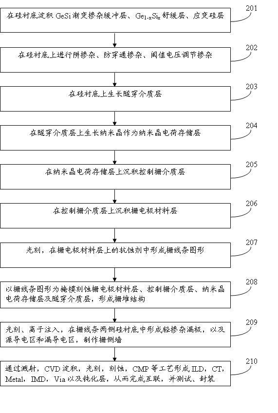
[0057] In order to make the object, technical solution and advantages of the present invention clearer, the present invention will be described in further detail below in conjunction with specific embodiments and with reference to the accompanying drawings.
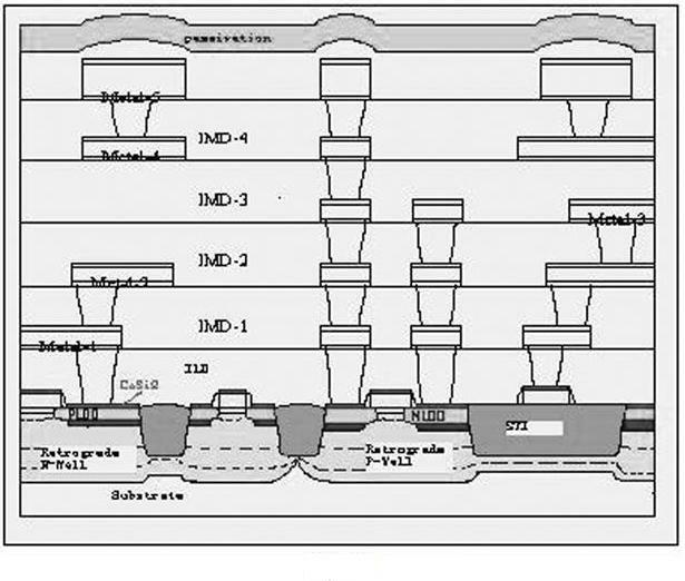
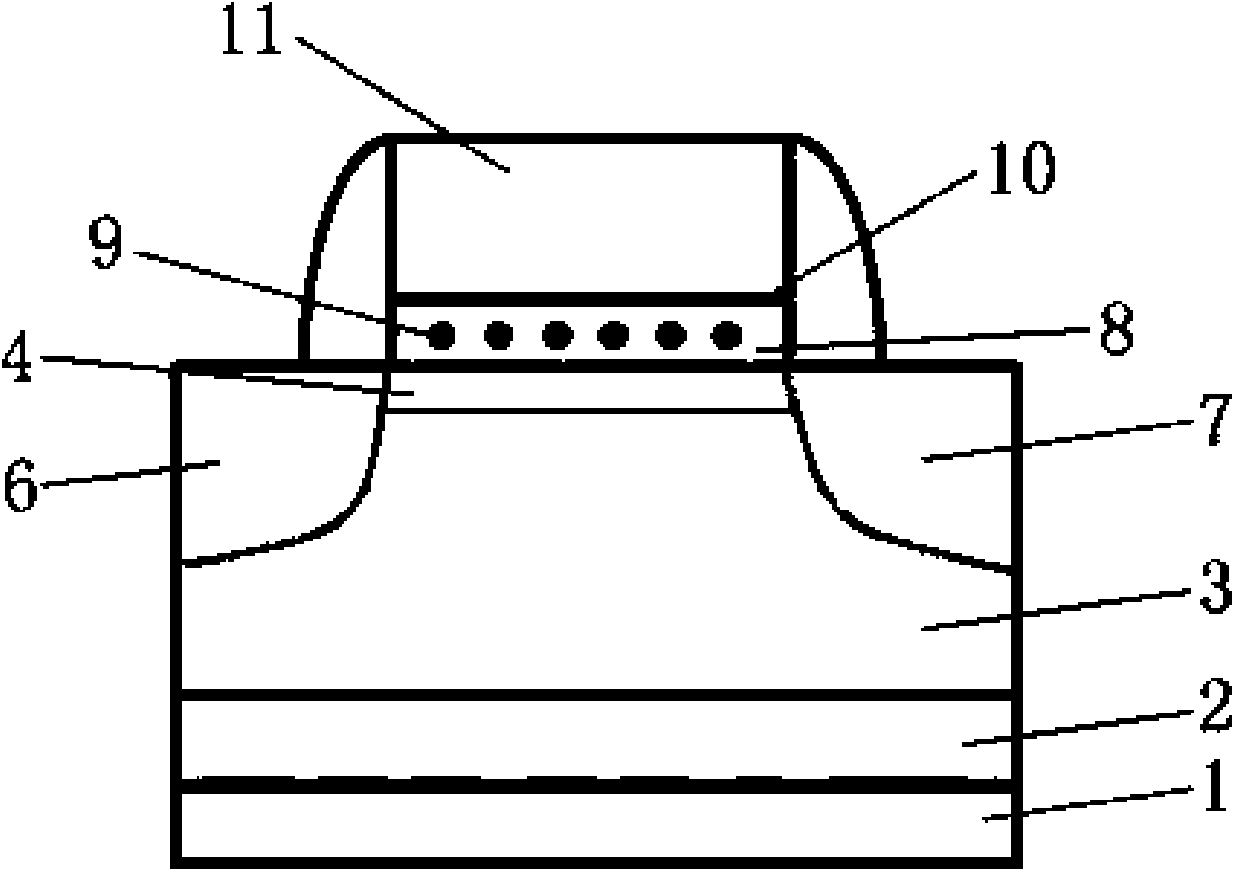
[0058] Such as figure 1 as shown, figure 1 Schematic diagram of the structure of the strained silicon-based nanocrystalline non-volatile memory provided by the embodiment of the present invention, the strained silicon-based nanocrystalline non-volatile memory includes a silicon substrate 1, deposited on the silicon substrate 1 GeSi gradient doped Impurity buffer layer 2, Ge 1-x Si x The relief layer 3 and the strained silicon layer 4 are located on the lightly doped drain, the source conduction region 6 and the drain conduction region 7 on both sides of the silicon substrate, and on the carrier channel between the source conduction region 6 and the drain conduction region 7 Covered tunnel dielectric layer 8, nanocrysta...
PUM
| Property | Measurement | Unit |
|---|---|---|
| Thickness | aaaaa | aaaaa |
| Diameter | aaaaa | aaaaa |
| Thickness | aaaaa | aaaaa |
Abstract
Description
Claims
Application Information