Preset cavity type SOI (silicon on insulator) substrate film bulk acoustic wave resonator and manufacturing method thereof

A thin-film bulk acoustic wave and manufacturing method technology, applied to electrical components, impedance networks, etc., can solve problems such as device failure, complex manufacturing process, and difficult control of precision, and achieve the effect of easy integration and simplified process steps

Inactive Publication Date: 2011-07-13
CHINA ELECTRONICS TECH GRP NO 26 RES INST
View PDF10 Cites 15 Cited by
  • Summary
  • Abstract
  • Description
  • Claims
  • Application Information

AI Technical Summary

Problems solved by technology

The cavity is the key to the formation of FBAR performance, and the manufacturing process is quite complicated. Its patents (US6060818, US6377137, US20050088257A1) mentioned that it needs to etch shallow grooves on the silicon wafer, fill the grooves with sacrificial layers, and CMP (chemical mechanical polishing) The key processes such as polishing the sacrificial layer and the release of the final sacrificial layer are prone to the following problems: (1) The sacrificial layer is thicker, with a thickness of several microns, and it is easy to form residual stress during the coating process by filling it with a coating, which will affect the next step of sacrificial layer CMP. Polishing and the release of the sacrificial layer have an impact; (2) The process of removing a few microns of the sacrificial layer by CMP on the entire silicon wafer surface (especially large-sized silicon wafers) is very complicated, and the accuracy is difficult to control. The requirements for the technical level of personnel are quite high; (3) The release process of the sacrificial layer is also relatively complicated. Considering the volume and size of the sacrificial layer, the release takes a long time. If the release is not complete, a complete cavity cannot be formed. If the release time is longer, the sacrificial layer releases the etchant and will cause some damage to the transducer; (4) During the release process of the sacrificial layer, adhesion may also occur in the cavity Phenomenon, which directly affects the yield of the device
This process has the following difficulties. (1) This method requires extremely high stress control technology in the coating process, and it is not easy to master; (2) During the release process of the sacrificial layer, the surroundings of the sacrificial layer, especially the upper and lower surfaces, are completely covered by electrodes and silicon wafers. Surrounding, it takes a long time to release all of them, and the release of etching solution from the sacrificial layer will cause damage to the transducer to some extent; (3) The steps at the edge of the sacrificial layer are not smooth enough, and the film thickness of the piezoelectric layer and its electrodes is between Distortion occurs here, which will cause stress concentration and break the transducer, causing hidden dangers to the reliability of the device

Method used


Image

  • Preset cavity type SOI (silicon on insulator) substrate film bulk acoustic wave resonator and manufacturing method thereof
  • Preset cavity type SOI (silicon on insulator) substrate film bulk acoustic wave resonator and manufacturing method thereof
  • Preset cavity type SOI (silicon on insulator) substrate film bulk acoustic wave resonator and manufacturing method thereof

Examples


Embodiment Construction

[0039] The preferred embodiments of the present invention will be described in detail below in conjunction with the accompanying drawings; it should be understood that the preferred embodiments are only for illustrating the present invention, rather than limiting the protection scope of the present invention.

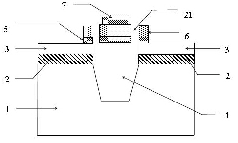
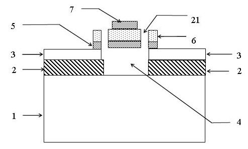
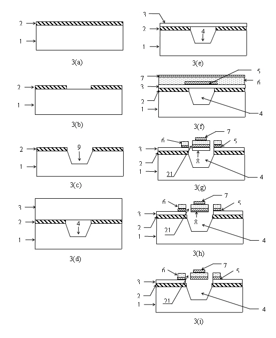
[0040] figure 1 It is a schematic diagram of the section structure of Embodiment 1 of the present invention, as shown in the figure: the pre-set cavity type SOI substrate thin film bulk acoustic resonator provided by the present invention includes a pre-set cavity type 4 SOI substrate and an SOI substrate An on-chip transducer, the transducer includes a bottom electrode 5, a top electrode 7, and a piezoelectric film 6 arranged between the bottom electrode 5 and the top electrode 7, the bottom electrode 5 is combined with the SOI substrate, and the The overlapping area of ​​the bottom electrode 5 , the top electrode 7 and the piezoelectric film 6 is opposite to the prede...


PUM


Abstract

The invention discloses a preset cavity type SOI (silicon on insulator) substrate film bulk acoustic wave resonator and a manufacturing method thereof, relating to the field of electronic devices. The acoustic wave resonator comprises a cavity SOI substrate and a piezoelectric film transducer arranged on the cavity SOI substrate, wherein the resonator comprises a piezoelectric film, a base electrode and a top electrode; the electrodes of the resonator are approximate to oval; a groove is arranged on the surface of a substrate silicon wafer in the cavity SOI substrate; and a closed cavity structure is formed by a top silicon and the substrate silicon wafer after bonding. Since a preset cavity structure is adopted, no sacrifice layer is used in the resonator and a chemical mechanical polishing process and a sacrifice layer releasing process for treating the sacrifice layers in foreign patents and products are unnecessary. Moreover, the preset cavity type SOI substrate film bulk acoustic wave resonator combines the advantages of SOI material, such as small source and drain parasitic capacitances, low voltage, low power consumption and the like. The resonator provided by the invention is compatible with an IC (integrated circuit), is easily integrated, is manufactured with simple process and is suitable for batch production.

Description

technical field [0001] The invention relates to the field of microelectronic devices, in particular to a thin-film bulk acoustic wave resonator and a manufacturing method. Background technique [0002] Film Bulk Acoustic Resonator (FBAR) is a device that uses acoustic resonance to achieve electrical frequency selection. The basic working principle of FBAR: When an electrical signal is loaded on the FBAR, the piezoelectric film in the device converts the electrical signal into an acoustic signal through the inverse piezoelectric effect, and the specific acoustic structure of the device presents selectivity for acoustic signals of different frequencies. Realize the function of frequency regulation. [0003] The rapid development of wireless communication technology (such as mobile communication, wireless sensor network) and radar technology requires more and more high-performance integrated microwave oscillators and duplex filters, which are used in signal sources and RF fron...

Claims


Application Information

Patent Timeline
Patent Type & Authority Applications(China)
IPC IPC(8): H03H9/54H03H3/02
Inventor 杨增涛马晋毅冷俊林赵建华杨正兵江洪敏傅金桥张龙周益民
Owner CHINA ELECTRONICS TECH GRP NO 26 RES INST
Why Eureka
Try Eureka