

Voltage zero-crossing detecting circuit and DC-DC converter with same
A detection circuit and voltage zero-crossing technology, applied in the direction of output power conversion devices, measuring current/voltage, instruments, etc., can solve the problems of difficult integration, large volume, expensive, etc., and achieve improved conversion efficiency, simple circuit structure, and energy saving area effect
- Summary
- Abstract
- Description
- Claims
- Application Information
AI Technical Summary
Problems solved by technology
Method used
Image

Examples
Embodiment 1
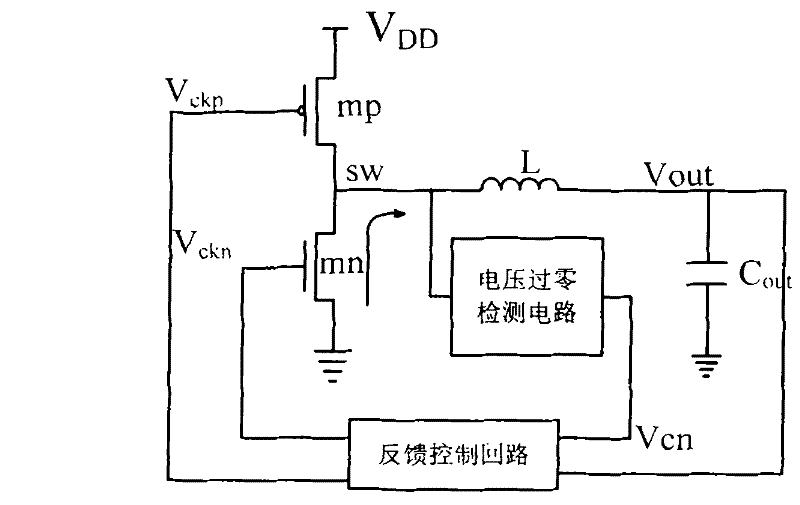
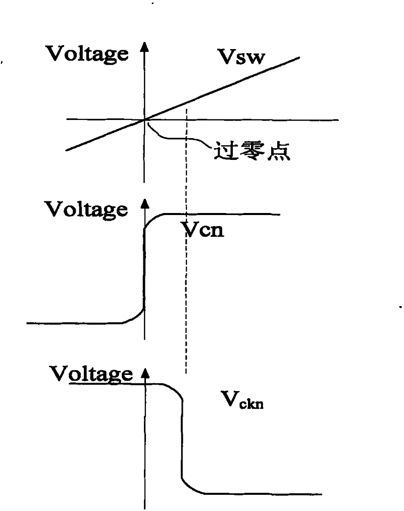
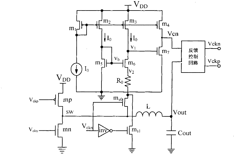
[0028] In the first embodiment, the voltage zero-crossing detection circuit adopts such as image 3 Described circuit structure, this structure comprises PMOS tube m 1 、m 2 、m 3 、m 4 , NMOS tube m 5 、m 6 、m 7 , switch tube m s0 、m s1 , inverter inv, current source I 0 and resistance R 0 , supply voltage V DD , the following combination as figure 1 The shown DC-DC converter illustrates the connection relationship of the voltage zero-crossing detection circuit described in this embodiment and the working principle applied to the DC-DC converter: wherein, the current source I 0 As a reference current source, it provides bias current to the amplifier, when V ckn When it is at a high level, the synchronous rectifier mn is turned on, and the inductance L is freewheeling, and the freewheeling direction is from the ground to the drain SW of the rectifier mn, and the voltage at the drain SW is input to the PMOS transistor m 3 、m 4 and NMOS tube m 6 、m 7 Composed of ampl...
Embodiment 2
[0043] Such as Figure 5 Shown is another voltage zero-crossing detection circuit of the present invention, the circuit structure is as follows image 3 On the basis of the voltage zero-crossing detection circuit shown, 5 PMOS transistors are added 8 、m 9 、m 10 、m 11 、m 12 and a reference current source I 0 , where the PMOS tube m 8 , PMOS tube m 9 , PMOS tube m 10 , PMOS tube m 11 Mirror connection, and in series with the PMOS transistor m 1 , PMOS tube m 2 , PMOS tube m 3 , PMOS tube m 4 source and supply V DD between, forming a folded current source structure; PMOS tube m 12 and reference current source I 0 in series with the power supply V DD and ground, and the PMOS tube m 12 The gate drain is connected to the PMOS tube m 1 、m 2 、m 3 、m 4 Provide bias voltage to ensure that the four PMOS tubes are in a deep saturation state; PMOS tube m 8 The gate and PMOS tube m 1 The drain is connected to the mirrored PMOS transistor m 8 、m 9 、m 10 、m 11 Provi...
Embodiment 3
[0046] Such as Image 6 Shown is another voltage zero-crossing detection circuit of the present invention, which removes the second-stage amplifier on the basis of the voltage zero-crossing detection circuit described in Embodiment 1, that is, removes the PMOS tube m 4 and NMOS tube m 7 , directly from the output terminal V of the first-stage amplifier 1 As V in Example 1 cn Output to the feedback control loop. The working principle of this circuit for detecting zero-crossing voltage is the same as that of the circuit shown in Embodiment 1. The gain of the one-stage amplifier is smaller than that of the two-stage amplifier, but the circuit structure is simple and the chip area is saved.
PUM
 Abstract
Description
Claims
Application Information