Supercharge Your Innovation With Domain-Expert AI Agents!

Luminous element and manufacturing method and luminous method thereof

A technology for light-emitting elements and manufacturing methods, which is applied to electrical components, semiconductor devices, circuits, etc., can solve the problems of limited application of light-emitting thin film materials, low light-emitting efficiency, weak light-emitting brightness, etc., and achieve broad production and application prospects and improve internal quantum efficiency. , the effect of spontaneous emission enhancement

Inactive Publication Date: 2011-07-20
OCEANS KING LIGHTING SCI&TECH CO LTD +1
View PDF0 Cites 3 Cited by
  • Summary
  • Abstract
  • Description
  • Claims
  • Application Information

AI Technical Summary

Problems solved by technology

However, the cerium-doped yttrium silicate thin film has the problems of weak luminous brightness and low luminous efficiency, which greatly limits the application of this light-emitting thin film material.

Method used


Image

  • Luminous element and manufacturing method and luminous method thereof
  • Luminous element and manufacturing method and luminous method thereof
  • Luminous element and manufacturing method and luminous method thereof

Examples


Embodiment 1

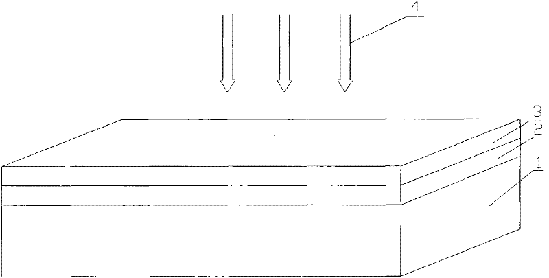
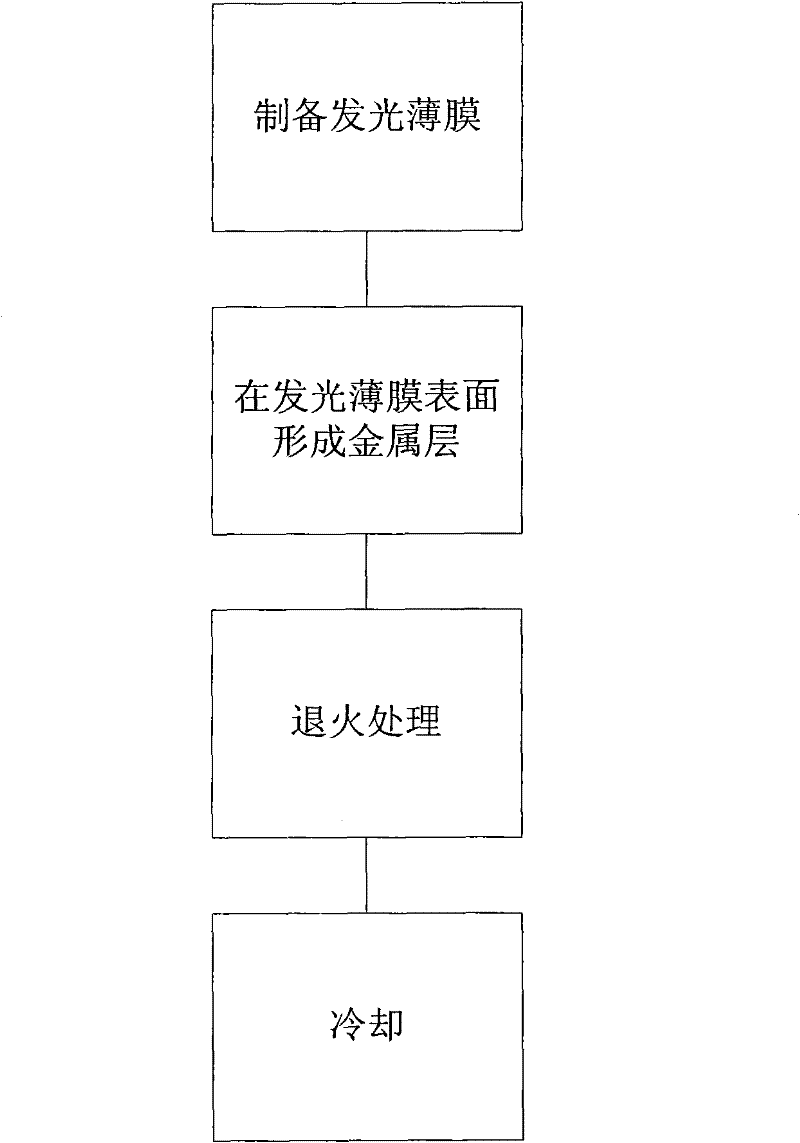
[0040] Select the size as 1×1cm 2 A double-sided polished quartz light-transmitting substrate is formed on the light-transmitting substrate by magnetron sputtering 1.99 Ce 0.01 SiO 5 Luminescent thin film, then use magnetron sputtering equipment to deposit a metal silver layer with a thickness of 2nm on the surface of the film, and then place it in a vacuum of 1×10 -3 Under a vacuum environment of Pa, annealing treatment was performed at a temperature of 300° C. for 30 minutes, and finally cooled to room temperature to obtain the light-emitting element of this embodiment.

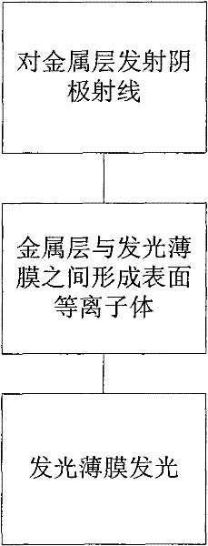
[0041] Figure 4 It is a comparison chart of the luminescence spectrum of the luminescent element of this embodiment and the luminescent film without metal layer using yttrium silicate doped with cerium system, wherein the test condition of the luminescence spectrum under cathode ray excitation is: the accelerating voltage of electron beam excitation is 5KV. Such as Figure 4 As shown, 11 is the lumine...

Embodiment 2

[0043] Select the size as 1×1cm 2 A double-sided polished quartz light-transmitting substrate is formed on the light-transmitting substrate by electron beam evaporation 1.998 Ce 0.002 SiO 5 Luminescent thin film, then using magnetron sputtering equipment to deposit a metal gold layer with a thickness of 0.5nm on the surface of the luminescent thin film, and then place it in a vacuum of 0.5×10 -3 Under a vacuum environment of Pa, annealing treatment was performed at a temperature of 200° C. for 60 minutes, and finally cooled to room temperature to obtain the light-emitting element of this embodiment.

Embodiment 3

[0045] Select the size as 1×1cm 2 A double-sided polished sapphire light-transmitting substrate, on which Y 1.995 Ce 0.005 SiO 5 Luminescent thin film, then use magnetron sputtering equipment to deposit a metal aluminum layer with a thickness of 200nm on the surface of the luminescent thin film, and then place it in a vacuum of 0.6×10 -4 Under a vacuum environment of Pa, annealing treatment was performed at a temperature of 500° C. for 300 min, and finally cooled to room temperature to obtain the light-emitting element of this embodiment.


PUM

PropertyMeasurementUnit
Thicknessaaaaaaaaaa

Abstract

The invention discloses a luminous element and a manufacturing method and a luminous method thereof. The luminous element comprises a luminous film and a metal layer, wherein the luminous film is made of a material having a chemical formula of Y2-xCexSiO5, x is more than 0 and less than or equal to 0.2; and the metal layer is positioned on the surface of the luminous film and has a metal microscopic structure. The manufacturing method comprises the following steps of: preparing the luminous film; preparing the metal layer on the luminous film, and annealing to make the metal layer have the metal microscopic structure; and finally, cooling to obtain the luminous element. When the luminous element emits light, cathode rays are transmitted to the metal layer, and a surface plasma is formed between the metal layer and the luminous film, so that the luminous film emits light. The manufacturing method is simple and low in cost; and the obtained luminous element is simple in structure, and has excellent luminous uniformity and stability, and the luminous efficiency is greatly improved.

Description

technical field [0001] The invention relates to the technical field of luminescent materials, in particular to a luminescent element, a manufacturing method thereof, and a luminescent method. Background technique [0002] Flat panel displays have always been the focus of research, and field emission displays are one of them. Since Ken Shoulder proposed the idea of ​​cathode ray micro-device based on field emission cathode arrays (FEAs) in the 1960s, the research on designing and manufacturing flat panel display and light source devices using FEAs has attracted great interest. Although its working principle is similar to that of a traditional cathode ray tube (CRT), it uses cathode rays to bombard red, green, and blue three-color phosphors to emit light for imaging or lighting purposes, but this device has advantages in brightness, viewing angle, response time, There are potential advantages in terms of operating temperature range, energy consumption, etc. [0003] At prese...

Claims


Application Information

Patent Timeline
IPC IPC(8): H01L33/44
Inventor 周明杰唐晶马文波
Owner OCEANS KING LIGHTING SCI&TECH CO LTD
Features
  • R&D
  • Intellectual Property
  • Life Sciences
  • Materials
  • Tech Scout
  • Unparalleled Data Quality
  • Higher Quality Content
  • 60% Fewer Hallucinations
Learn More