Circuit structure for reducing input offset voltage of two-stage operational amplifier

A technology of operational amplifiers and offset voltages, applied in differential amplifiers, DC-coupled DC amplifiers, etc., can solve the problems of increasing circuit area and circuit complexity, and achieve the goals of reducing input offset voltage, low power consumption, and reducing offsets Effect

Active Publication Date: 2011-07-20
XIAN JIEHANG ELECTRONICS SCI & TECH CO LTD
View PDF4 Cites 18 Cited by
  • Summary
  • Abstract
  • Description
  • Claims
  • Application Information

AI Technical Summary

Problems solved by technology

The current circuit design idea of ​​reducing the offset voltage of the op amp is realized by using chopper technology and automatic zero adjustment technology, but the chopper technology needs to couple the input signal with the switch-type square wave signal, and then obtain it after synchronous demodulation and low-pass filtering. For small non-linear signals, the circuit complexity increases, which will significantly increase the circuit area; the automatic zeroing technology needs to store the offset in the capacitor, mainly including input offset storage and output offset storage, and is mainly suitable for discrete signal circuits such as switched capacitors.

Method used


Image

  • Circuit structure for reducing input offset voltage of two-stage operational amplifier
  • Circuit structure for reducing input offset voltage of two-stage operational amplifier
  • Circuit structure for reducing input offset voltage of two-stage operational amplifier

Examples


Embodiment Construction

[0017] The present invention will be described in detail below in conjunction with the accompanying drawings and specific embodiments.

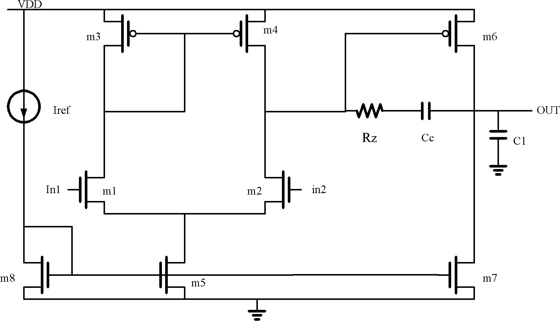
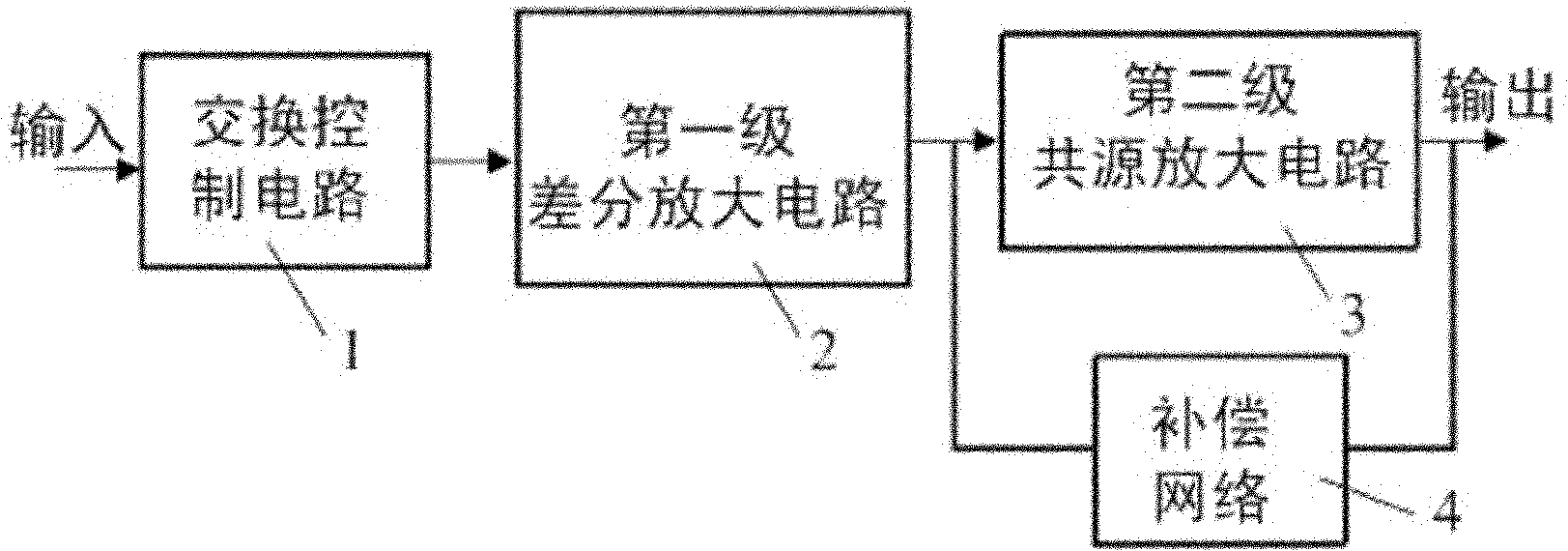
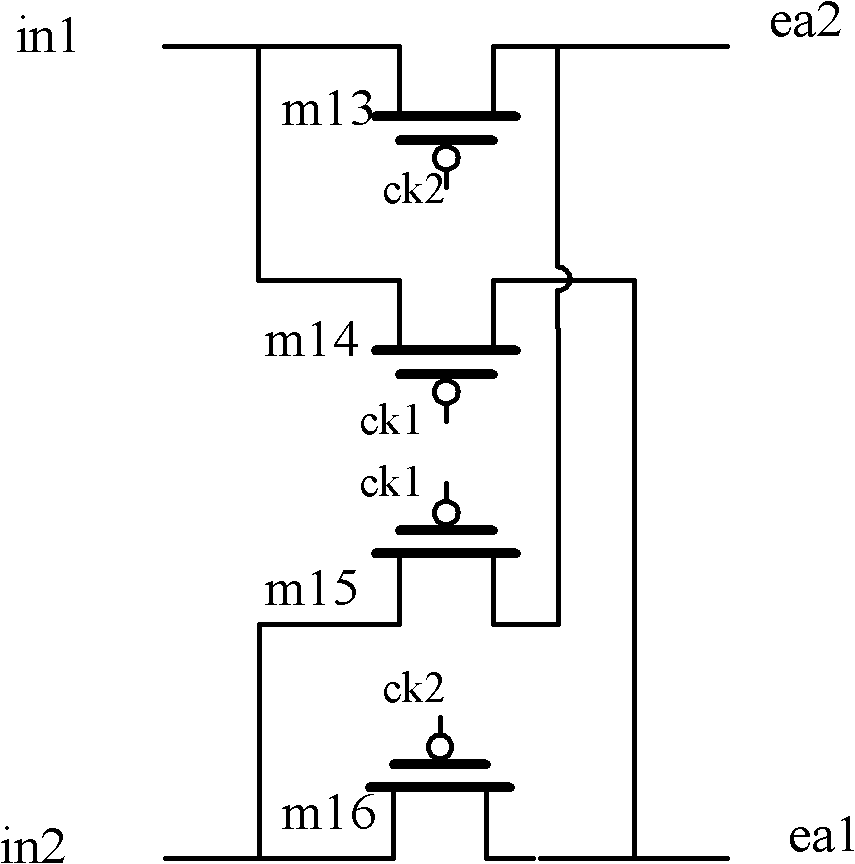
[0018] Such as figure 1 As shown, the traditional two-stage operational amplifier circuit includes a first-stage ordinary differential amplifier circuit, a second-stage common-source amplifier circuit and a compensation network; the first-stage ordinary differential amplifier circuit consists of a first NMOS transistor m1, a second NMOS transistor m2, The third NMOS transistor m5 is composed of the first PMOS transistor m3 and the second PMOS transistor m4. The second-stage common source amplifier circuit is composed of the fourth NMOS transistor m7 and the seventh PMOS transistor m6. The compensation network includes a series zero-suppressing resistor R z and compensation capacitor C c . In addition, the reference current source I ref and the fifth NMOS transistor m8 provide mirror currents for the third NMOS transistor m5 and the fourth ...


PUM


Abstract

The invention provides a circuit structure for reducing input offset voltage of a two-stage operational amplifier, which comprises a switching control circuit, a first-stage differential amplification circuit, a second-stage common-source amplification circuit and a compensation network, wherein the output end of the switching control circuit is connected with the input end of the first-stage differential amplification circuit, the output end of the first-stage differential amplification circuit is connected with the input end of the second-stage common-source amplification circuit, and the compensation network is further connected between the input end and the output end of the second-stage common-source amplification circuit. The circuit structure has the benefits that the offset of theoperational amplifier is reduced by adopting an MOS (metal oxide semiconductor) switching tube to control and exchange signals at the positive and the negative input ends and the signals at the output end of the operational amplifier; as only the MOS switching tube is increased in the circuit, the circuit structure only needs very small area and very low power consumption; and the circuit does not affect the gain of the operational amplifier, the phase margin, the power supply voltage rejection ratio, the common-mode input range and other performance indexes while reducing the input offset voltage of the operational amplifier, and can be applied in mainstream CMOS (complementary metal oxide semiconductor) circuit systems.

Description

technical field [0001] The invention belongs to the technical field of microelectronics and solid electronics, relates to an operational amplifier circuit of an integrated circuit, and in particular relates to a circuit structure for reducing the input offset voltage of a two-stage operational amplifier. Background technique [0002] Operational amplifiers are widely used in analog circuits and digital-analog hybrid circuits. Since CMOS technology has become the mainstream technology of integrated circuits, CMOS operational amplifier circuits have significant advantages in cost and development cycle compared with traditional bipolar circuits. The current circuit design idea of ​​reducing the offset voltage of the op amp is realized by using chopper technology and automatic zero adjustment technology, but the chopper technology needs to couple the input signal with the switch-type square wave signal, and then obtain it after synchronous demodulation and low-pass filtering. F...

Claims


Application Information

Patent Timeline
Patent Type & Authority Applications(China)
IPC IPC(8): H03F3/45
Inventor 杨媛杨晓菲
Owner XIAN JIEHANG ELECTRONICS SCI & TECH CO LTD
Why Eureka
Try Eureka