

Method for manufacturing 6-inch POWERMOS transistor epitaxial layer
A manufacturing method and epitaxial layer technology, which are applied in semiconductor/solid-state device manufacturing, electrical components, circuits, etc., can solve the problems of reducing the effective thickness of the epitaxial layer, decreasing the yield of the device, and poor uniformity, so as to suppress the self-doping phenomenon. , Consistency improvement, the effect of improving electrical performance and yield
- Summary
- Abstract
- Description
- Claims
- Application Information
AI Technical Summary
Problems solved by technology
Method used
Image


Examples
Embodiment Construction
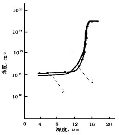
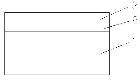
[0026] A method for manufacturing the epitaxial layer of a 6-inch POWERMOS tube, which is characterized in that it is carried out according to the following steps:
[0027] 1) Select the appropriate POWERMOS tube substrate 1 and perform certain pre-treatment;
[0028] 2) Perform HCL vapor phase etching on the substrate at a certain temperature;
[0029] 3) Perform the first H 2 Variable speed purge;
[0030] 4) Deposit a non-doped intrinsic layer 2 with a thickness of 1-2 um on the substrate;
[0031] 5) Perform the second H 2 Variable speed purge;
[0032] 6) A second epitaxial layer 3 is formed on the intrinsic layer.
[0033] The equipment used in the present invention is a PE-2061S epitaxial furnace produced in Italy, which is heated by high-frequency induction mode, and the base is made of high-purity graphite surface subjected to cracking treatment and covered with a layer of high-purity SiC.
[0034] Reaction chamber, substrate sheet cleaning and graphite base treatment: When the re...
PUM
 Abstract
Description
Claims
Application Information