Silicon solar cell and manufacturing method thereof

A technology of silicon solar cells and silicon wafers, applied in the manufacture of circuits, electrical components, final products, etc., can solve the problems of small photovoltaic power generation, high cost and large-scale application of photovoltaic power generation, achieve small contact resistance, avoid battery current drop, The effect of preventing undercutting

Active Publication Date: 2011-08-17
CECEP SOLAR ENERGY TECH
View PDF4 Cites 13 Cited by
  • Summary
  • Abstract
  • Description
  • Claims
  • Application Information

AI Technical Summary

Problems solved by technology

At present, the proportion of photovoltaic power generation in energy is very small, and the high

Method used


Image

  • Silicon solar cell and manufacturing method thereof
  • Silicon solar cell and manufacturing method thereof
  • Silicon solar cell and manufacturing method thereof

Examples


Embodiment Construction

[0028] The present invention will be described in detail below in conjunction with the accompanying drawings and embodiments.

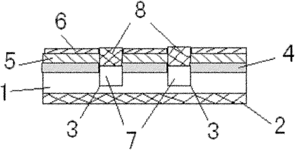
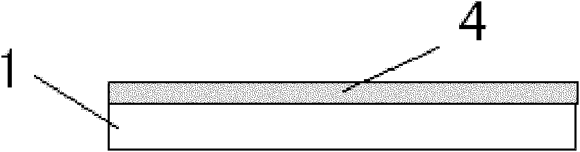
[0029] Such as figure 1 As shown, the silicon solar cell of the present invention includes a silicon wafer 1, and the back side of the silicon wafer 1 is provided with a Ti / Pd / Ag electrode 2 to form a back electrode; the front side of the silicon wafer 1 is uniformly provided with two grooves 3 by etching, and N-type silicon 4 , oxide layer 5 and ITO (indium tin oxide) film 6 are sequentially arranged on the front of silicon wafer 1 , and the shapes of N-type silicon 4 , oxide layer 5 and ITO film 6 are all corresponding to silicon wafer 1 . In the two grooves 3, N + Type silicon 7 and Ti / Pd / Ag electrode 8, two Ti / Pd / Ag electrodes 8 form the positive electrode.

[0030] In the above embodiment, the silicon wafer 1 is a P-type radial double-sided polished silicon wafer with a resistivity of 3 Ωcm and a thickness of 320 μm.

[0031] In the above-men...


PUM

PropertyMeasurementUnit
Sheet resistanceaaaaaaaaaa
Thicknessaaaaaaaaaa

Abstract

The invention relates to a silicon solar cell and a manufacturing method thereof. the method comprises the following steps: (1) carrying out wet-type chemical cleaning on a silicon wafer, and drying; (2) carrying out single-side phosphorus source diffusion on the silicon wafer; (3) placing the silicon wafer into an oxide furnace, and forming an oxide layer; (4) carrying out primary photoetching on the frontage of the silicon wafer; (5) removing the oxide layer of the photoetching graphics part of the silicon wafer; (6) carrying out whirl coating protection on the diffusion surface of the silicon wafer, and then corroding the oxide layer at the back surface; (7) carrying out single-side phosphorus source anew partial diffusion on the silicon wafer; (8) removing the oxide layer at the back surface of the silicon wafer; (9) evaporating a Ti/Pd/Ag electrode on the back surface of the silicon wafer, and then annealing; (10) firstly carrying out whirl coating protection on the back surface of the silicon wafer, and removing an optical resist at the back surface of the silicon wafer; (11) evaporating an indium tin film at the frontage of the silicon wafer by utilizing a magnetic control sputtering device; (12) carrying out secondary photoetching on the frontage of the silicon wafer; (13) carrying out tertiary photoetching on the frontage of the silicon wafer; and (14) removing the optical resist at the frontage of the silicon wafer, and annealing. According to the invention, the cell conversion efficiency can be improved effectively; and the cell and method provided by the invention can be widely used in the field of solar cells.

Description

technical field [0001] The invention relates to a solar cell and a preparation method thereof, in particular to a silicon solar cell and a preparation method thereof. Background technique [0002] Energy and environment are two basic issues facing mankind in the 21st century. The development of pollution-free and renewable new energy is the only way to solve these two problems. At present, the proportion of photovoltaic power generation in energy is very small, and the high cost is the main obstacle restricting the large-scale application of photovoltaic power generation. Developing a new generation of high-efficiency, low-cost solar cells that generate electricity at a cost close to or even lower than conventional energy sources has become a top priority. The traditional battery manufacturing process is: cleaning texturing - diffusion - dephosphorization silicon etching - deposition of silicon nitride - silk screen sintering. Since the technological conditions of each pr...

Claims


Application Information

Patent Timeline
IPC IPC(8): H01L31/18H01L31/0352H01L31/0224
CPCY02P70/50
Inventor 勾宪芳曹华斌姜利凯王鹏宋爽
Owner CECEP SOLAR ENERGY TECH
Why Eureka
Try Eureka