Film transistor, electronic equipment and manufacture method thereof

A technology of thin-film transistors and electronic equipment, which is applied in semiconductor/solid-state device manufacturing, circuits, electrical components, etc. It can solve the problems of large size, performance fluctuations such as mobility and switching ratio, and easy deterioration of active layer characteristics, so as to achieve stable performance. , the effect of improving performance

Inactive Publication Date: 2011-08-24
SONY CORP
View PDF8 Cites 4 Cited by
  • Summary
  • Abstract
  • Description
  • Claims
  • Application Information

AI Technical Summary

Problems solved by technology

In this case, if the organic TFT is excessively heated in the packaging process, the characteristics of the active layer are likely to deteriorate, and therefore, there is a high possibility that performance fluctuations such as mobility and switching ratio will occur in the organic TFT.

Method used


Image

  • Film transistor, electronic equipment and manufacture method thereof
  • Film transistor, electronic equipment and manufacture method thereof
  • Film transistor, electronic equipment and manufacture method thereof

Examples


Embodiment 1~4

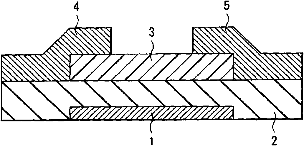
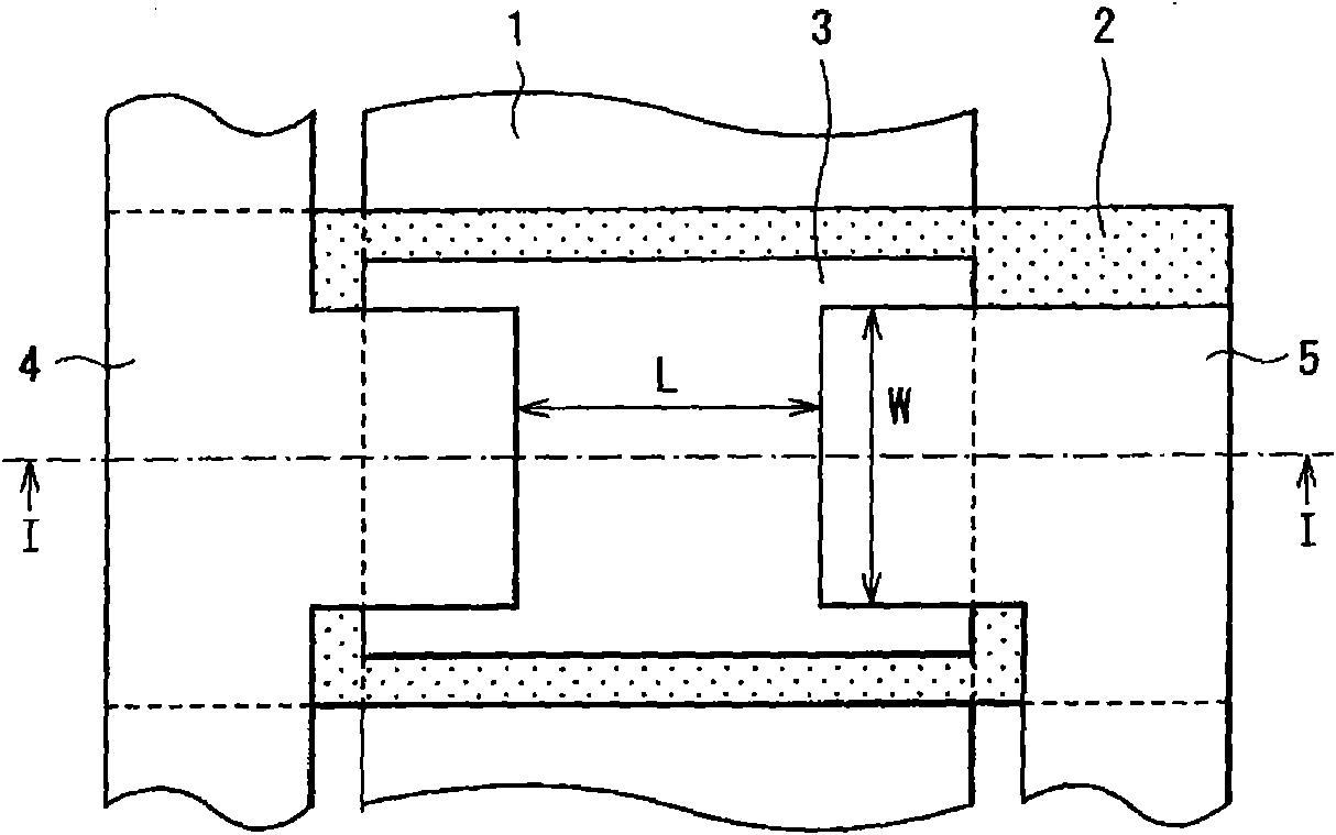
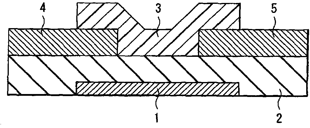
[0098] An experimental organic TFT of bottom-gate bottom-contact type was fabricated and its performance was studied. In the case of making organic TFTs, a silicon wafer doped with boron (B), phosphorus (P), antimony (Sb), or arsenic (As) is prepared first as a substrate for the gate electrode function. Then, a silicon dioxide (SiO 2 ) Constitute a gate insulating layer (thickness=150nm). Next, source and drain electrodes made of gold are formed on the gate insulating layer. In this case, make figure 2 The dimensions (L, W) shown are L=50μm and W=30mm. Next, the soluble organic semiconductor materials and soluble polymer materials (glass transition temperature Tg: °C) shown in Table 1 were dissolved in toluene to prepare a solution. In this case, the mixing ratio (weight ratio) of the soluble organic semiconductor material and the soluble polymer material is 1:1, and the total solid content is 1% by weight. As the soluble organic semiconductor material, a dioxaneanthanthren...


PUM


Abstract

The invention provides a film transistor, an electronic equipment and a manufacture method thereof. The stable performance is ensured by the film transistor. Organic TFT comprises a grid electrode (1), an active layer (3) arranged opposite to the grid electrode (1) and separated by a grid insulating layer (2), a source electrode (4) and a leakage electrode (5) separated from each other and connected with the active layer (3). The active layer (3) comprises soluble organic semi-conducting material and soluble macromolecular material. The vitrification temperature of the soluble macromolecular material is higher than the highest temperature during the packaging process.

Description

Technical field [0001] The present invention relates to a thin film transistor including an active layer containing an organic semiconductor material, an electronic device using the thin film transistor, and a manufacturing method thereof. Background technique [0002] In recent years, field effect transistors (FET: Field Effect Transistor) have been used in various technical fields, and among them, thin film transistors (TFT: Thin Film Transistor) have been widely used. This TFT is installed in many electronic devices, for example, used as a pixel selection device in active matrix displays. [0003] The TFT connects the source electrode and the drain electrode with an active layer (a so-called channel layer), which is separated from the gate electrode via a gate insulating layer. In the TFT, the current flowing between the source electrode and the drain electrode is controlled according to the voltage applied to the gate electrode, and the current flows while accumulating or cons...

Claims


Application Information

Patent Timeline
Patent Type & Authority Applications(China)
IPC IPC(8): H01L51/05H01L51/30H01L51/40
Inventor 福田敏生大江贵裕
Owner SONY CORP
Why Eureka
Try Eureka