Internal gettering process of Czochralski silicon wafer

A Czochralski silicon wafer and process technology, applied in the direction of crystal growth, electrical components, circuits, etc., can solve problems such as reducing thermal budget, and achieve the effect of reducing thermal budget, temperature and time

Active Publication Date: 2011-08-31
ZHEJIANG UNIV
View PDF4 Cites 12 Cited by
  • Summary
  • Abstract
  • Description
  • Claims
  • Application Information

AI Technical Summary

Problems solved by technology

However, the thermal budget of the very large-scale integrated circuit process has a tendency to decrease continuously, so the internal gettering process of Czochralski silicon wafers also needs to be further reduced

Method used


Image

  • Internal gettering process of Czochralski silicon wafer
  • Internal gettering process of Czochralski silicon wafer
  • Internal gettering process of Czochralski silicon wafer

Examples


Embodiment 1

[0020] (1) The diameter is 300mm, the crystal orientation is , and the interstitial oxygen concentration is 8×10 17 cm -3 The Czochralski silicon wafers are subjected to rapid thermal treatment (RTP) under a high-purity (purity greater than 99.99%) nitrogen atmosphere. The conditions are: the temperature is raised to 1250°C at a rate of 100°C / s, maintained for 60 seconds, and then heated at a rate of 5°C / s Cool at a rate of 800°C, then cut off the power supply to allow the silicon wafer to cool naturally;

[0021] (2) Annealing the silicon wafer treated in step (1) at 900° C. for 8 hours under an argon atmosphere.

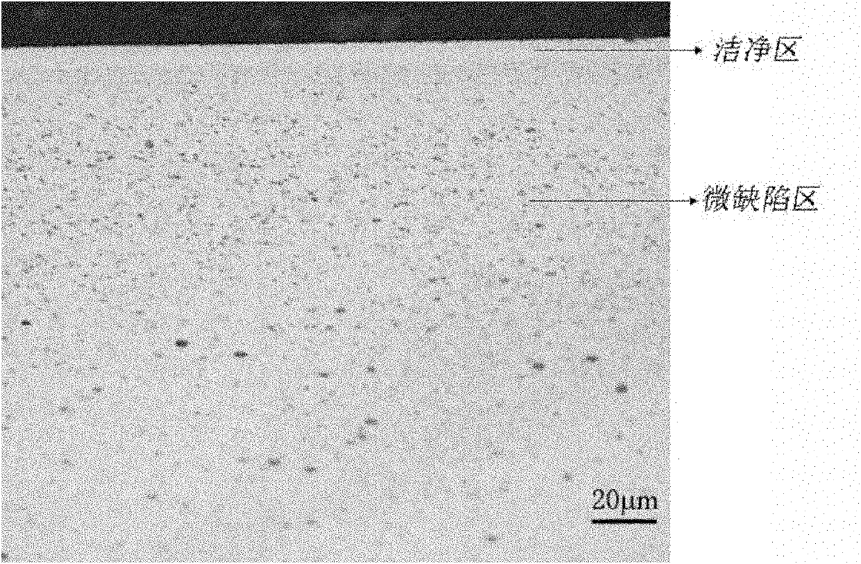
[0022] figure 1 It is an optical microscope photo of the silicon wafer section obtained after the treatment in Example 1 after preferential etching. From figure 1 It can be seen that a defect-free clean area is formed near the surface of the silicon wafer, and a dense bulk micro-defect area is next to it below it, which will play the role of internal gettering....

Embodiment 2

[0024] (1) The diameter is 200mm, the crystal orientation is , and the interstitial oxygen concentration is 8×10 17 cm -3 The Czochralski silicon wafer is subjected to rapid thermal treatment (RTP) in a high-purity nitrogen atmosphere. The conditions are: heating up to 1200°C at a rate of 100°C / s, maintaining for 120 seconds, and then cooling to 1000°C at a rate of 50°C / s. Then cut off the power supply to let the silicon wafer cool down naturally;

[0025] (2) Annealing the silicon wafer treated in step (1) at 900° C. for 16 hours under an argon atmosphere.

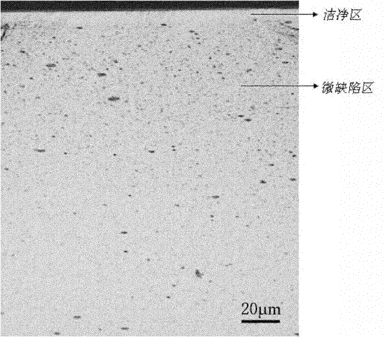
[0026] The effect after implementation is similar to that of Example 1, and the silicon wafer includes a clean area and a bulk micro-defect area.

Embodiment 3

[0028] (1) The diameter is 300mm, the crystal orientation is , and the interstitial oxygen concentration is 9×10 17 cm -3 The Czochralski silicon wafers were subjected to rapid thermal treatment (RTP) under a nitrogen atmosphere. The conditions were: heating up to 1200 °C at a rate of 100 °C / s, maintaining for 150 seconds, and then cooling to 1000 °C at a rate of 5 °C / s, and then Cut off the power supply and let the silicon wafer cool down naturally;

[0029] (2) Annealing the silicon wafer treated in step (1) at 900° C. for 16 hours under an argon atmosphere.

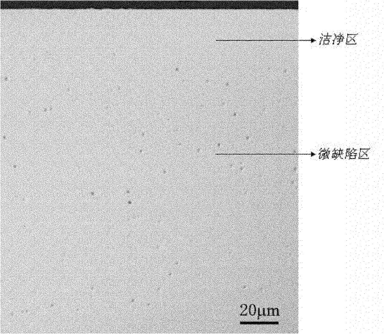
[0030] figure 2 It is an optical microscope photo of the silicon wafer section obtained after Example 3 after preferential etching. From figure 2 It can be seen that a defect-free clean area is formed near the surface of the silicon wafer, and a dense bulk micro-defect area is next to it below it, which will play the role of internal gettering.


PUM

PropertyMeasurementUnit
diameteraaaaaaaaaa

Abstract

The invention discloses an internal gettering process of a Czochralski silicon wafer, which comprises the following steps of: (1) in nitrogen atmosphere, heating the Czochralski silicon wafer at a speed of 50-100 DEG C / sec to 1200-1250 DEG C, holding for 30-150 seconds, and then cooling the Czochralski silicon wafer at a speed of 5-50 DEG C / sec to 800-1000 DEG C, and naturally cooling; and (2) annealing the Czochralski silicon wafer after being treated in the step (1) in argon atmosphere at a temperature of 800-900 DEG C for 8 to 16 hours. The invention only comprises a two-step heat treatment process, the required temperature and time are lower than those of the traditional process, and the heat budget is obviously reduced; and in addition, the concentration of bulk micro-defect and the width of a clean zone can be conveniently controlled by the temperature, time and cooling speed of rapid heat treatment of the first step.

Description

technical field [0001] The invention relates to a gettering process for silicon wafers, in particular to an internal gettering process for Czochralski silicon wafers. Background technique [0002] Czochralski silicon wafer is the basic material of integrated circuits. One of the fundamental reasons is that Czochralski silicon wafer has internal gettering ability related to oxygen precipitation. Integrated circuits will inevitably encounter metal contamination during the manufacturing process. If the metal contamination in the active region of the device cannot be eliminated, the manufacturing yield of integrated circuits will drop significantly. In order to solve this problem, high-density oxygen precipitation and its induced defects are usually formed in the silicon wafer (this area is called the bulk micro-defect region); and the near-surface area of ​​the silicon wafer (ie: the active area of ​​the device) Oxygen precipitation does not form (this area is called clean zon...

Claims


Application Information

Patent Timeline
Patent Type & Authority Applications(China)
IPC IPC(8): C30B33/02C30B29/06
CPCC30B33/02C30B29/06H01L21/322H01L21/3225
Inventor 马向阳徐泽王彪杨德仁
Owner ZHEJIANG UNIV
Why Eureka
Try Eureka