Method for epitaxially growing strontium titanate (STO) thin film on gallium arsenide (GaAs) substrate
An epitaxial growth, gallium arsenide-based technology, applied in the field of materials, can solve the problems of complex methods, high growth temperature, damage to GaAs semiconductor characteristics, etc., and achieve the effect of high thermodynamic stability and uniformity, and smooth film surface.
- Summary
- Abstract
- Description
- Claims
- Application Information
AI Technical Summary
Problems solved by technology
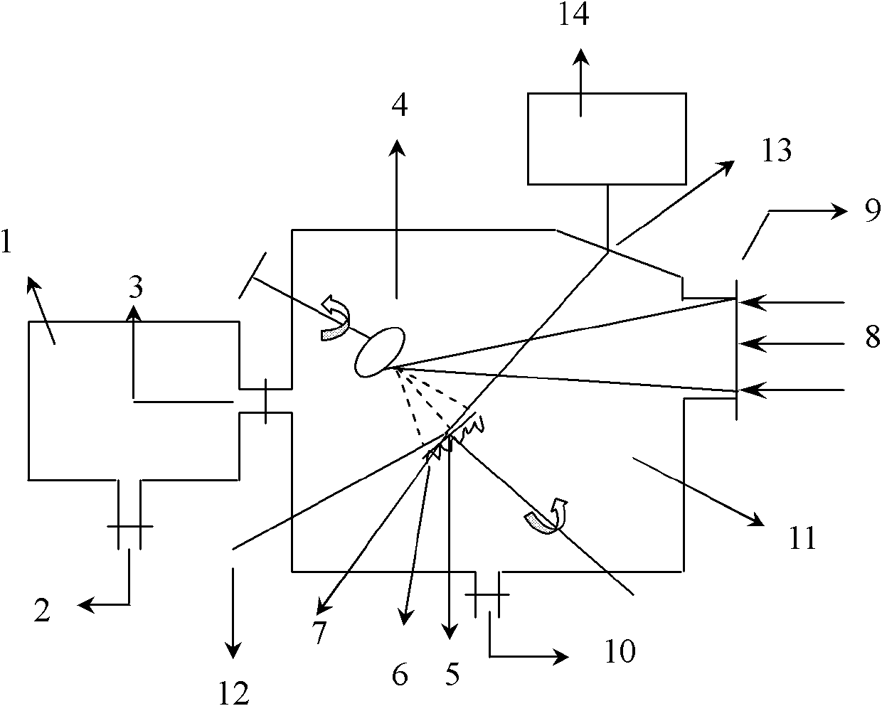
Method used
Image

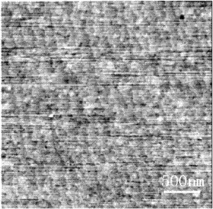
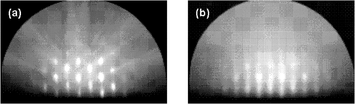
Examples
Embodiment Construction
[0020] The present invention will be further described below in conjunction with the accompanying drawings and specific embodiments.
[0021] A strontium titanate thin film epitaxially grown on a gallium arsenide substrate, the specific steps are as follows:
[0022] Step 1: Perform surface treatment on the GaAs substrate to form a clean surface with atomically flat Ga atoms as the terminal surface.
[0023] The specific process of this step in this embodiment is as follows: surface treatment of the GaAs substrate, first ultrasonic cleaning in trichlorethylene solution for 5 minutes, then ultrasonic cleaning in acetone solution for 5 minutes, and then ultrasonic cleaning in alcohol solution for 5 minutes ; Then wash in deionized water for 5 minutes; use HF (hydrofluoric acid) solution (such as HF: H 2 O=1:50) to clean for 1 minute, remove the oxide layer on the surface of the substrate, and use N 2 The substrate was blown dry, and sent into the MBE cavity for in-situ N (nitr...
PUM
| Property | Measurement | Unit |
|---|---|---|
| electron mobility | aaaaa | aaaaa |
| surface roughness | aaaaa | aaaaa |
| dielectric loss | aaaaa | aaaaa |
Abstract
Description
Claims
Application Information