III-group nitride light-emitting diode (LED) and manufacturing method thereof

A technology of light-emitting diodes and manufacturing methods, which is applied in the direction of electrical components, circuits, semiconductor devices, etc., can solve the problems of increasing the complexity and uncertainty of the LED manufacturing process, improve crystal quality and uniformity of light emission, improve crystal quality, The effect of improving reliability

Active Publication Date: 2011-09-14
SUN YAT SEN UNIV
View PDF8 Cites 19 Cited by
  • Summary
  • Abstract
  • Description
  • Claims
  • Application Information

AI Technical Summary

Problems solved by technology

[0006] Looking at these methods of improving current expansion, or introducing non-traditional insertion layers, or using unconventional process methods, all of which increase the complexity and uncertainty of the LED manufacturing process, which is not conducive to the realization of large-scale industrialization.

Method used


Image

  • III-group nitride light-emitting diode (LED) and manufacturing method thereof
  • III-group nitride light-emitting diode (LED) and manufacturing method thereof
  • III-group nitride light-emitting diode (LED) and manufacturing method thereof

Examples


Embodiment 1

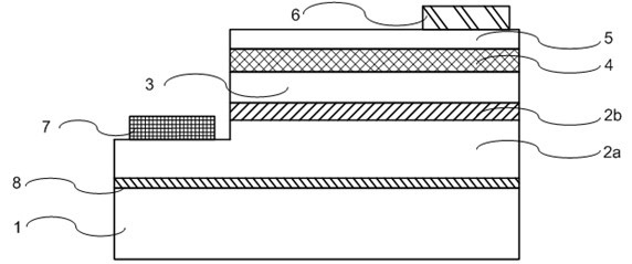
[0032] Such as figure 1 As shown, a III-nitride light-emitting diode includes a substrate 1 and a semiconductor epitaxial stack stacked on the substrate. The above-mentioned substrate 1 is made of sapphire (Al 2 o 3 ) material, the semiconductor epitaxial stack is made of aluminum gallium indium nitrogen (In x Ga y Al 1-x-y N, 0<=x<=1, 0<=y<=1) material formation. In order to solve the lattice mismatch problem between the semiconductor epitaxial stack and the substrate, a buffer layer 8 is provided between the semiconductor epitaxial stack and the substrate.

[0033] The semiconductor epitaxial stack includes an N-type layer 2, a light-emitting layer 3, and a P-type layer 4 from bottom to top. Part of the semiconductor epitaxial stack is etched to form an N-type layer mesa in the N-type layer 2. The N-type layer mesa N-type electrode 7 is arranged on it; P-type electrode 6 is arranged on the upper surface of the unetched part of P-type layer 4; The heterogeneous layer 2b, ...

Embodiment 2

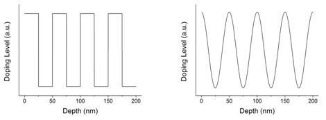
[0044] Such as image 3 As shown, the difference between this embodiment and Embodiment 1 is that the modulation doped layer 2b in the N-type layer 2 of the light-emitting diode of this embodiment is a gradient transition layer with a concentration, and the doping concentration of the uniform doped layer gradually decreases. for low doping concentration. The doping concentration is controlled by the flow rate of metal organic chemical vapor deposition equipment for impurities during epitaxial growth. The modulation doped layer 2 b is a doping linearly changing region with a thickness of 50 nm, and the closer to the light-emitting layer 3 , the lower the doping concentration. During the manufacturing process, the doping method can be changed to a non-linear monotonically decreasing form according to actual requirements, and the thickness of the modulation doping layer 2b can also be changed accordingly.


PUM


Abstract

The invention discloses a III-group nitride light-emitting diode (LED) and a manufacturing method thereof. The LED comprises a substrate and a semiconductor epitaxial laminate which is laminated on the substrate, wherein the semiconductor epitaxial laminate sequentially comprises an N type layer, a luminescent layer and a P type layer from top to bottom. The LED is characterized in that: an N type layer table face is formed in the N type layer by etching a part of the semiconductor epitaxial laminate; an N type electrode is arranged on the N type layer table face; a P type electrode is arranged on the upper surface of the un-etched part of the P type layer; the N type layer also comprises a uniformly doped layer of which the doping concentration is consistent and a modulation doped layer of which the doping concentration is changeable; and the modulation doped layer is arranged between the uniformly doped layer and the luminescent layer. A doped mode of the modulation doped layer is gradual transition doping which connects uniformly doped layer and the luminescent layer of which the doping concentration is consistent. The concentration change trend is decrease progressively change from the uniformly doped layer to the luminescent layer. By the LED and the manufacturing method, the crystal quality and the luminance uniformity can be obviously improved, and the lighting effect is improved.

Description

technical field [0001] The invention relates to a light-emitting diode, in particular to a high-power Group III nitride light-emitting diode and a manufacturing method thereof. Background technique [0002] In the past two decades, GaN-based materials have been greatly developed in epitaxial growth and device technology, making III-nitride semiconductor materials widely used in blue / green and white light-emitting diodes, ultraviolet detectors and high-power electronic devices; In particular, currently, LED devices based on InGaN / GaN quantum wells have entered the commercialization level. Due to the extremely high cost of self-supporting GaN substrates, the homoepitaxial growth of GaN materials is extremely difficult; therefore, currently widely used substrate materials include sapphire (Al 2 o 3 ), SiC and Si. Compared with other materials, although sapphire has disadvantages such as non-conductivity and poor thermal conductivity, it has become the mainstream GaN substrat...

Claims


Application Information

Patent Timeline
Patent Type & Authority Applications(China)
IPC IPC(8): H01L33/14H01L33/00
Inventor 王钢江灏郑致远
Owner SUN YAT SEN UNIV
Why Eureka
Try Eureka