Integrated touch display device and making method thereof
A touch display and liquid crystal display technology, applied in the field of integrated touch display devices, can solve the problems of difficult control of the manufacturing process, low electrode resolution, and low production efficiency, so as to reduce the processing steps, increase the visible area, and improve the processing efficiency Effect
- Summary
- Abstract
- Description
- Claims
- Application Information
AI Technical Summary
Problems solved by technology
Method used
Image
Examples
Embodiment 1
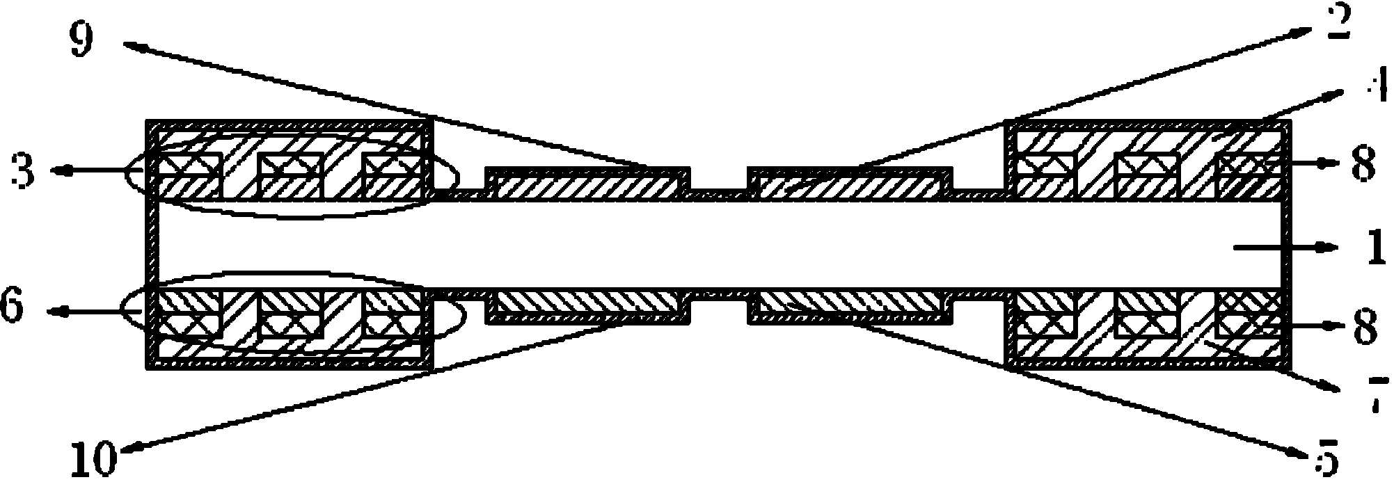
[0049] The roll-type polyethylene terephthalate (PET) film is selected as the base material, and an indium tin oxide (ITO) layer 2 and a copper (Cu) layer are successively plated on the upper surface of the PET film 1 by vacuum sputtering coating method 8, and then successively plate indium tin oxide (ITO) layer 5 and copper (Cu) layer 8 on the lower surface by vacuum sputtering coating method, see image 3 ; Make photosensitive adhesive layer 11 and layer 12 successively with the mode of screen printing on both sides, refer to Figure 4 , and then expose, develop, etch, and remove glue at one time, and make transparent electrode patterns and wiring strengthening patterns at the same time, see Figure 5 , 6, 7; then make protective adhesive layer 4 and layer 7 by screen printing in the area where the wiring is strengthened, see Figure 8 ; This protective glue needs to be able to withstand the immersion of the secondary etching solution; then, perform a second round of second...
Embodiment 2
[0051] The difference between this embodiment and Embodiment 1 is that the base material used for sensor production is not only PET, but also glass, or PC, or PMMA, or polyolefin, or flexible materials.
Embodiment 3
[0053] The difference between this embodiment and Embodiment 1 is that, in addition to using the method of vacuum sputtering coating to make the transparent conductive layer, it can also be made by vacuum ion coating, vacuum thermal evaporation coating or coating. The transparent conductive layer can be indium tin oxide (ITO), zinc oxide (ZnO), tin oxide (SnO), aluminum (Al), nickel (Ni), molybdenum (Mo), gold (Au), silver (Ag), copper (Cu), carbon nanotube (CNT) film or conductive resin or any combination of several.
PUM
| Property | Measurement | Unit |
|---|---|---|
| thickness | aaaaa | aaaaa |
Abstract
Description
Claims
Application Information


