Preparation technology for silicon nano-aperture array photovoltaic material and photovoltaic cell

A technology of photovoltaic cells and photovoltaic materials, which is applied in the fields of circuits, electrical components, and final product manufacturing, and can solve the problems of unstable battery structure and low photoelectric conversion efficiency.

Inactive Publication Date: 2011-09-28
BEIJING NORMAL UNIVERSITY
View PDF12 Cites 12 Cited by
  • Summary
  • Abstract
  • Description
  • Claims
  • Application Information

AI Technical Summary

Problems solved by technology

However, due to obvious defects such as the p-n junction preparation technology and the instability of the cell stru

Method used


Image

  • Preparation technology for silicon nano-aperture array photovoltaic material and photovoltaic cell
  • Preparation technology for silicon nano-aperture array photovoltaic material and photovoltaic cell

Examples


specific Embodiment approach 1

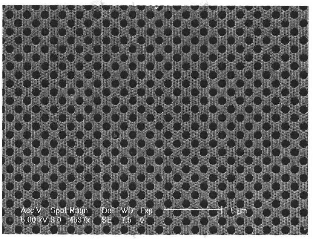
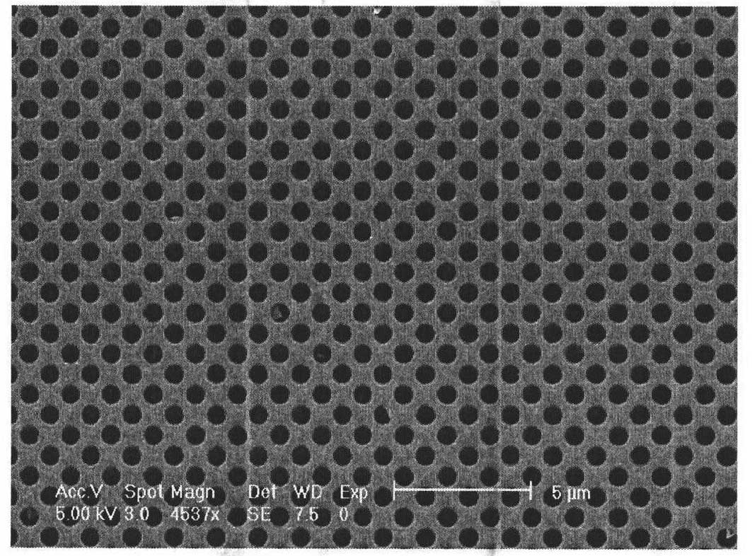
[0021] Using deep ultraviolet lithography technology and high vacuum metal deposition technology to obtain a large area of ​​the same size and periodically distributed silver nanoparticle arrays on the surface of a clean silicon wafer; then immediately immerse the silicon wafer in a HF+H 2 o 2 +H 2 In an airtight container of O etching solution, treat at 25 degrees Celsius for 20 minutes to obtain a silicon nanohole array. The samples were then soaked in concentrated nitric acid solution for at least one hour to remove the silver film on the surface.

specific Embodiment approach 2

[0022] Using deep ultraviolet lithography technology and high-vacuum metal deposition technology to obtain a large area of ​​the same size and periodically distributed gold nanoparticle arrays on the surface of a clean silicon wafer; then immediately immerse the silicon wafer in a HF+H 2 o 2 +H 2 In an airtight container of O etching solution, treat at 25 degrees Celsius for 20 minutes to obtain a silicon nanohole array. The samples were then soaked in aqua regia solution for at least one hour to remove the gold film on the surface.

specific Embodiment approach 3

[0023] Deposit a uniformly distributed silver film on the surface of a clean silicon wafer using high-vacuum metal deposition technology, and then thermally anneal at 200 degrees Celsius under a nitrogen protective atmosphere to form a large-area array of silver nanoparticles with the same size and periodic distribution on the silicon surface; then immediately Immerse the silicon wafer in HF+H 2 o 2 +H 2 In an airtight container of O etching solution, treat at 25 degrees Celsius for 30 minutes to obtain a silicon nanohole array. The samples were then soaked in concentrated nitric acid solution for at least one hour to remove the silver film on the surface.


PUM


Abstract

The invention discloses a preparation technology for a silicon nano-aperture array photovoltaic material and photovoltaic cell. In the invention, a preparation method for a large-area highly-ordered silicon nano-aperture array is developed in the combination of a metal catalytic silicon corrosion technology and a photoetching technology or a nano self-assembly technology. The large-area highly-ordered silicon nano-aperture array structure has excellent antireflection and wide spectrum absorption performances, and is an excellent photovoltaic material.

Description

technical field [0001] The invention relates to a silicon nanometer hole array photovoltaic material and a photovoltaic cell preparation technology, belonging to the technical field of new materials and solar energy. Background technique [0002] In recent years, the potential crisis of energy and the deterioration of the ecological environment have forced countries all over the world to actively develop renewable and clean energy. Compared with other renewable energy sources, solar energy is superior in terms of the quantity of resources, the universality of distribution, cleanliness and technical reliability. A solar cell is a device that directly converts light energy into electrical energy through the photovoltaic effect of a semiconductor pn junction or a semiconductor-liquid junction. At present, commercial solar cells are mainly monocrystalline silicon, polycrystalline silicon and amorphous silicon [see patents: Patent No. JP5243597-A; -B1; Patent No. JP2002198549-A...

Claims


Application Information

Patent Timeline
IPC IPC(8): H01L31/18
CPCY02P70/50
Inventor 彭奎庆王新
Owner BEIJING NORMAL UNIVERSITY
Why Eureka
Try Eureka