Manufacturing method of sacrifice layer of MEMS (Micro-electromechanical System)

A manufacturing method and sacrificial layer technology, applied in microstructure technology, microstructure devices, manufacturing microstructure devices, etc., can solve the problems of affecting equipment, waste of silicon wafers, poor film contact, etc., to improve performance and enhance adhesion. , The effect of preventing peeling

Active Publication Date: 2011-10-05
SHANGHAI INTEGRATED CIRCUIT RES & DEV CENT
View PDF9 Cites 8 Cited by
  • Summary
  • Abstract
  • Description
  • Claims
  • Application Information

AI Technical Summary

Problems solved by technology

[0009] In the existing CMOS-MEMS single-chip integration technology, PECVD technology is used to utilize SiH 4 Decompose to form amorphous silicon, which is used to realize the silicon sacrificial layer film forming process, so as to be compatible with the CMOS process; because the sacrificial layer is required to be relatively thick, and the amorphous silicon film formed by this method has a very high H content, and the film is relatively loose , so it is not in good contact with the film formed in the previous process; at the same time, in the subsequent process, the H defects in the amorphous silicon film will continue to reunite and overflow with time and temperature, resulting in severe peeling of the subsequent film and the amorphous silicon film, resulting in silicon Disposal of the film, and will affect related equipment, causing cross-contamination problems

Method used


Image

  • Manufacturing method of sacrifice layer of MEMS (Micro-electromechanical System)
  • Manufacturing method of sacrifice layer of MEMS (Micro-electromechanical System)
  • Manufacturing method of sacrifice layer of MEMS (Micro-electromechanical System)

Examples


Embodiment Construction

[0029] In order to make the content of the present invention clearer and easier to understand, the content of the present invention will be described in detail below in conjunction with specific embodiments and accompanying drawings.

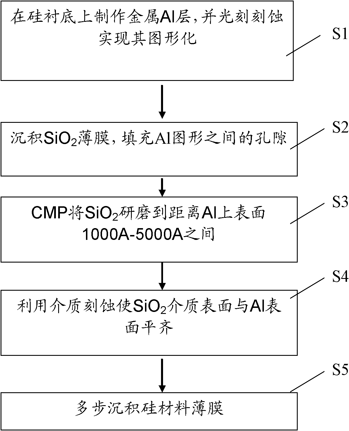
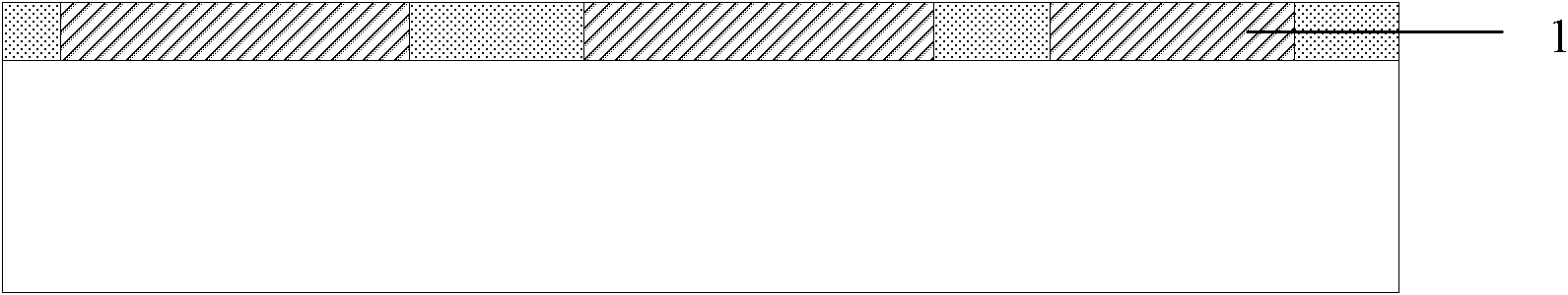
[0030] figure 1 A flow chart of a method for manufacturing a MEMS sacrificial layer structure according to an embodiment of the present invention is schematically shown. Simultaneously, Figure 2 to Figure 5 A schematic diagram of a semiconductor device structure obtained in each step of the MEMS sacrificial layer structure manufacturing method according to an embodiment of the present invention is shown.

[0031] Such as figure 1As shown, in step S1, a metal, such as metal aluminum, is formed on a silicon substrate, and then photolithography, etch, degrease, and cleaning are performed to realize its patterning. Preferably, after the patterning process of the front metal layer, the MEMS structure performs the surface treatment of the silicon ...


PUM


Abstract

The invention discloses a manufacturing method of a sacrifice layer of an MEMS (Micro-electromechanical System). The method comprises the following steps of: metal layer forming; silicon wafer surface processing before sacrifice layer deposition, used for improving the surface characteristics of a silicon wafer; supported hole patterning for patterning a supported hole in a sacrifice layer; and sacrifice layer postprocessing for processing the sacrifice layer to form a surface film on the surface of the sacrifice layer. The formed surface film covers the sacrifice layer effectively for solving the problem that the film strips off from the sacrifice layer because of H overflow, thereby improving the performance, the yield and the reliability of related MEMS products.

Description

technical field [0001] The invention relates to the technical field of MEMS manufacturing, in particular to a method for manufacturing a MEMS sacrificial layer structure. Background technique [0002] Micro-Electro-Mechanical System (MEMS) technology has many advantages such as tiny, intelligent, executable, integrable, good process compatibility, and low cost, so it has begun to be widely used in many fields. The MEMS micro-bridge structure is a very widely used structure in the MEMS field. It uses a sacrificial layer release process to form a bridge structure, which can be widely used in detectors, sensors and other products. The integration of CMOS and MEMS can combine the high performance of CMOS and the multi-function of MEMS, and become the key to promote the large-scale application of MEMS technology. [0003] The MEMS micro-bridge structure uses a sacrificial layer to realize the micro-bridge structure, and the sacrificial layer is removed by a release process after...

Claims


Application Information

Patent Timeline
Patent Type & Authority Applications(China)
IPC IPC(8): B81C1/00
Inventor 康晓旭左青云李佳青
Owner SHANGHAI INTEGRATED CIRCUIT RES & DEV CENT
Why Eureka
Try Eureka