Light-emitting diode (LED) epitaxial structure and manufacturing method thereof

A technology of light-emitting diodes and epitaxial structures, applied in electrical components, circuits, semiconductor devices, etc., can solve the problem that the performance and electrode structure of MQW and P-GaN materials are not enough to meet high-performance applications, and improve the ability to resist ESD, improve ESD level, the effect of avoiding ESD breakdown

Inactive Publication Date: 2011-10-05
中山大学佛山研究院 +1
View PDF7 Cites 19 Cited by
  • Summary
  • Abstract
  • Description
  • Claims
  • Application Information

AI Technical Summary

Problems solved by technology

[0005] One of the technical problems to be solved by the present invention is to provide a light-emitting diode epitaxial structure, which solves the problem that the performance and electrode structure of MQW and P-GaN materials in the prior art are not enough to meet the needs of high-performance application fields

Method used


Image

  • Light-emitting diode (LED) epitaxial structure and manufacturing method thereof
  • Light-emitting diode (LED) epitaxial structure and manufacturing method thereof
  • Light-emitting diode (LED) epitaxial structure and manufacturing method thereof

Examples


Embodiment Construction

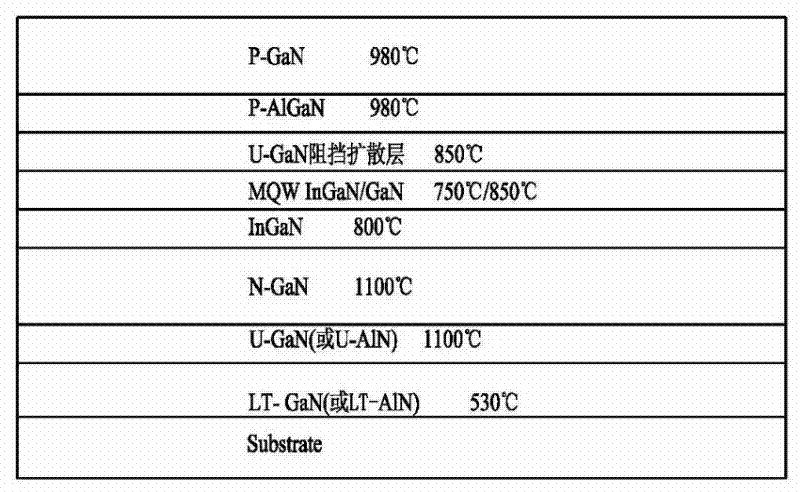
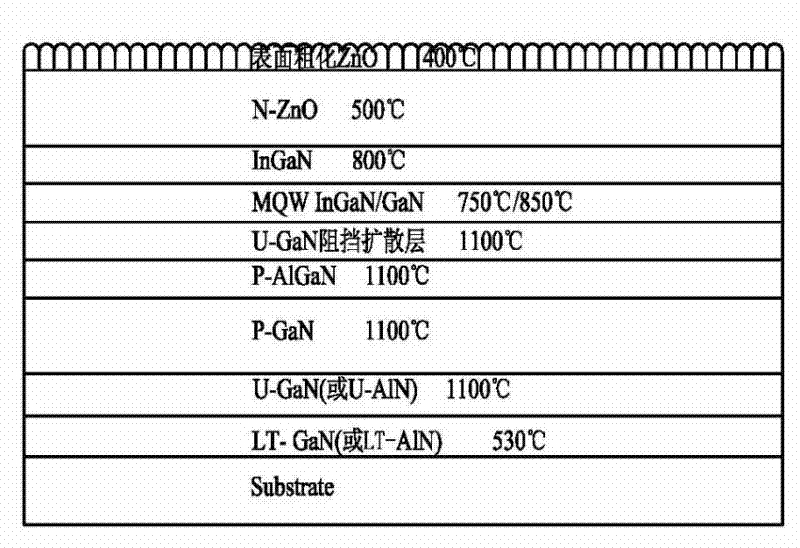
[0048] The purpose of this specific embodiment is to provide a novel light-emitting diode epitaxial structure and its manufacturing method. In short, the method uses an N-ZnO layer to replace the N-GaN layer in the existing light-emitting diode epitaxial structure, The LED epitaxial structure manufactured by this method is as image 3 As shown, its structure includes: low-temperature gallium nitride (LT-GaN) or aluminum nitride (AlN) nucleation layer grown sequentially on the epitaxial substrate material (Substrate layer), high-temperature non-doped gallium nitride or aluminum nitride Buffer layer (U-GaN layer or U-AlN layer), P-type gallium nitride layer (P-GaN layer), P-type gallium aluminum nitride layer (P-AlGaN layer), barrier diffusion layer of P layer and light emitting layer (U-GaN Barrier space layer), multi-quantum well light-emitting layer (MQW InGaN / GaN), InGaN current spreading layer (n-InGaN layer), N-type zinc oxide (N-ZnO) layer and surface roughened N-ZnO lay...


PUM

PropertyMeasurementUnit
thicknessaaaaaaaaaa
thicknessaaaaaaaaaa
thicknessaaaaaaaaaa

Abstract

The invention discloses a light-emitting diode (LED) epitaxial structure and a manufacturing method thereof. The LED epitaxial structure successively comprises an epitaxial substrate, a leukotriene (LT)-GaN nucleating layer, a high-temperature non-doped buffer layer, a P-GaN layer, a P-AlGaN layer, a diffusion barrier layer, a multiple quantum well (MQW) luminous layer, an InGaN current expansion layer, an N-ZnO layer and a surface-coarsened ZnO layer. The manufacturing method comprises the following steps: pre-treating the epitaxial substrate; growing the nucleating layer; growing the buffer layer; growing the P-GaN layer; growing the P-AlGaN layer; growing the diffusion barrier layer; growing the MQW luminous layer; growing the InGaN current expansion layer; growing the N-ZnO layer; and growing the surface-coarsened ZnO layer. By using the LED epitaxial structure obtained by virtue of the manufacturing method provided by the invention, an excellent electrical property and a good optical property are obtained, the internal quantum efficiency and the electronic static discharge (ESD) resistance capability are improved, the lost light caused by total reflection is lowered, the external quantum efficiency is greatly improved, a high-brightness LED is obtained, and the purposes of development and sustainable development of the LED industry are greatly promoted.

Description

technical field [0001] The invention relates to the technical field of semiconductor light-emitting diodes, in particular to an epitaxial structure of a light-emitting diode and a manufacturing method thereof, in particular to an epitaxial structure of a light-emitting diode in which N-GaN is replaced by N-ZnO and a manufacturing method thereof. Background technique [0002] Since the commercialization of GaN-LED (gallium nitride light-emitting diode) in the early 1990s, the application fields of LED products have rapidly expanded from signal indication, traffic lights, landscape lighting, automotive lighting, backlight sources to general lighting, etc. . [0003] Although the structure development of GaN-LED is becoming more and more mature, compared with the maturity of AlGaInP series materials, the quality of GaN-LED P-type materials is only barely usable. plus its such as figure 1 The sequentially grown epitaxial structure (Substrate / N-GaN / (InGaN / GaN) MQW / P-GaN LED) an...

Claims


Application Information

Patent Timeline
Patent Type & Authority Applications(China)
IPC IPC(8): H01L33/06H01L33/00H01L33/02
Inventor 王钢王孟源童存声
Owner 中山大学佛山研究院
Why Eureka
Try Eureka