Inorganic semiconductor nanometer material and preparation method thereof

A technology of inorganic semiconductors and nanomaterials, applied in the field of nanomaterials, can solve the problem of small size dependence, and achieve the effect of simple method and low cost

Inactive Publication Date: 2011-10-12
THE NAT CENT FOR NANOSCI & TECH NCNST OF CHINA
View PDF5 Cites 6 Cited by
  • Summary
  • Abstract
  • Description
  • Claims
  • Application Information

AI Technical Summary

Problems solved by technology

[0003] At present, researchers have synthesized small-sized chiral metal clusters (Chem.Soc.Rev.2009, 38, 757-771), and coordinated chiral molecules with nanoparticles for chiral molecular detection (Nat Biotech1999, 17, 371-374), but the optical characteristics and chiral characteristics of such small-sized metal clusters are less dependent on their size, thus limiting their application fields
In contrast, inorganic semiconductor nanoparticles have more obvious "size"-dependent optical and electrical characteristics, but there are no inorganic semiconductor nanomaterials with chiral characteristics

Method used


Image

  • Inorganic semiconductor nanometer material and preparation method thereof
  • Inorganic semiconductor nanometer material and preparation method thereof
  • Inorganic semiconductor nanometer material and preparation method thereof

Examples


Embodiment 1

[0035] [Example 1]: Preparation of chiral cadmium telluride nanoparticles

[0036] 1) Dissolve 0.5g of cadmium perchlorate (ie, cationic complexing agent) and 0.1g of D-cysteine ​​and L-cysteine ​​(ie, chiral stabilizer) in water, and adjust the pH value to 11 (Concrete method can refer to J.Phys.Chem.B 2002,106,7177-7185);

[0037] 2) Then introduce hydrogen telluride gas (i.e. anion complexing agent) under an inert atmosphere, heat at 80-100°C to grow CdTe, and then obtain D-cysteine-stabilized cadmium telluride nanoparticles and L-cysteine ​​stabilized cadmium telluride nanoparticles.

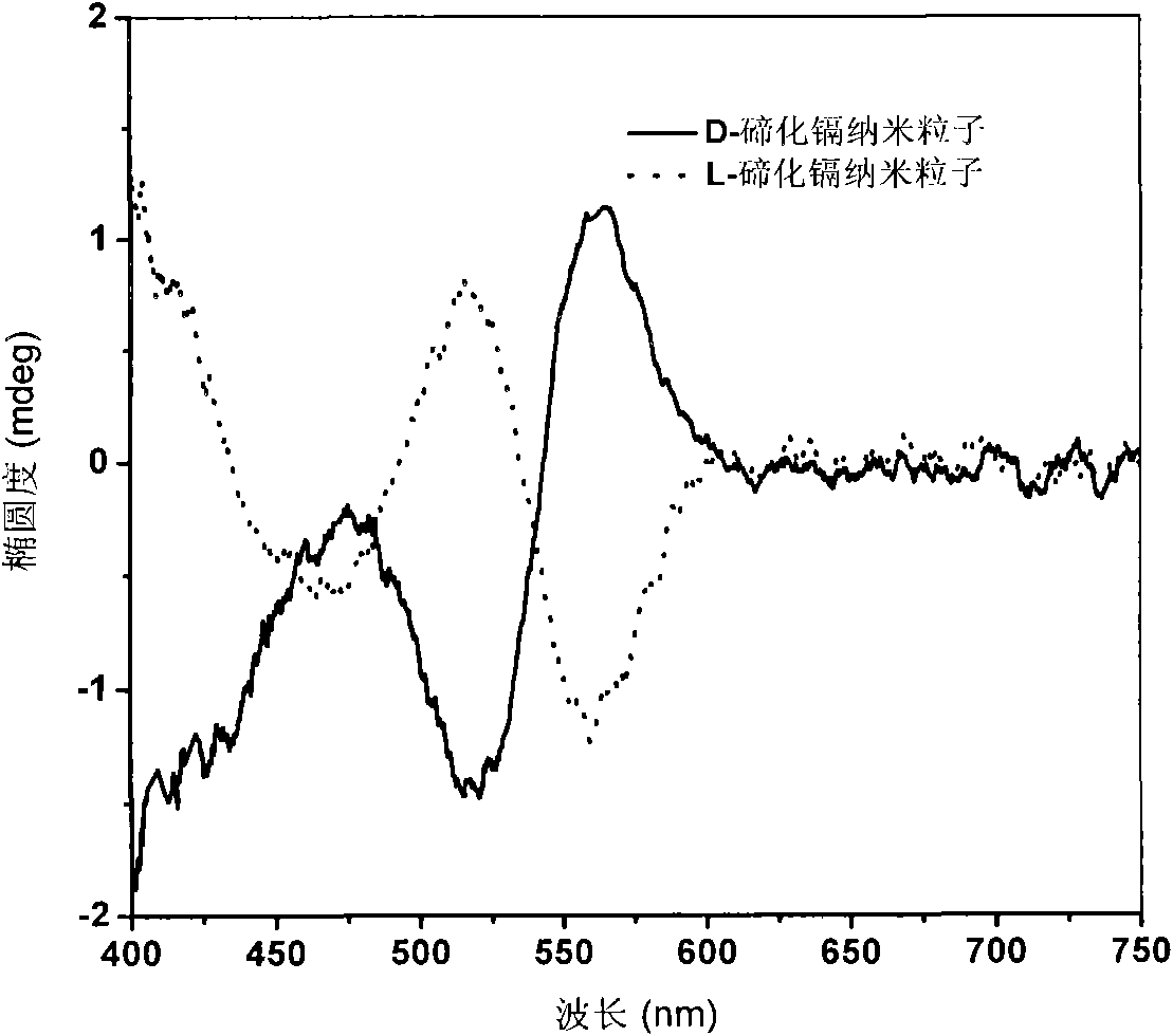
[0038] The chiral characteristics of materials are characterized by measuring the difference in absorption rate of chiral substances for left-handed and right-handed polarized light by circular dichroism spectroscopy. figure 1 Circular dichroism spectra of D-cadmium telluride and L-cadmium telluride chiral nanoparticles. From this figure, it can be seen that the circular dichroism spectra...

Embodiment 2

[0039] [Example 2]: Preparation of chiral tellurium cadmium sulfide alloy nanoparticles

[0040] 1) Weigh 0.5g cadmium perchlorate (ie, cationic complexing agent) and 0.6g L-glutathione (ie, chiral stabilizer), dissolve the above two substances in water, and adjust the pH value to 11.3;

[0041] 2) Then introduce hydrogen telluride gas (that is, the anion complexing agent) under an inert atmosphere, and heat at 100° C. to obtain chiral cadmium telluride sulfide alloy nanoparticles.

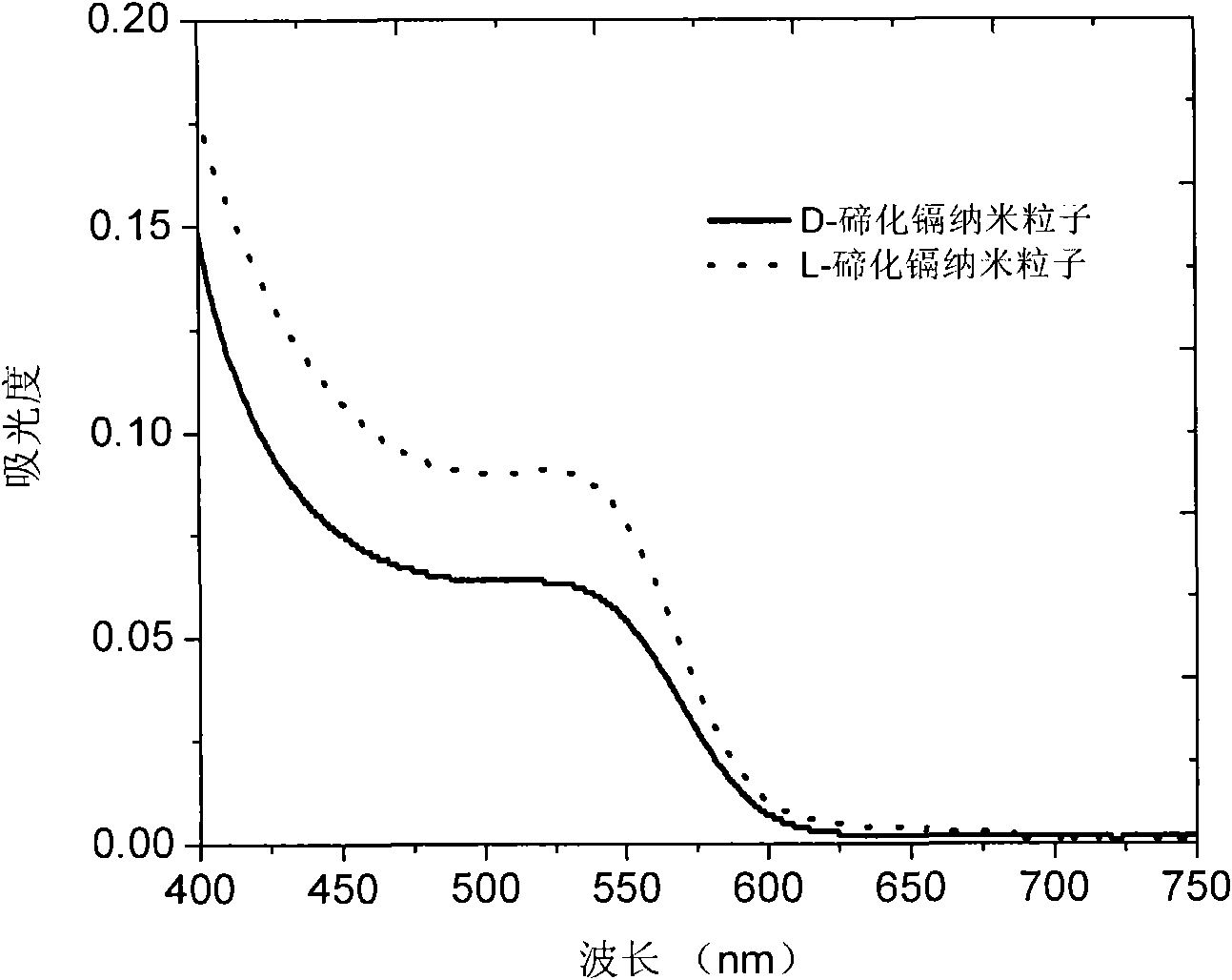
[0042] Figure 5 It is the circular dichroism spectrum and the ultraviolet-visible spectrum of chiral cadmium telluride sulfide. The two absorption peaks of the ultraviolet-visible spectrum are attributed to CdS and CdTe, and both of them have optical absorption in the circular dichroism spectrum. Image 6 The XRD pattern of the product reflects the structure characteristics of sphalerite of cadmium telluride sulfide. combine Figure 5 , Image 6 It can be seen that the obtained nanoparticles ...

Embodiment 3

[0043] [Example 3]: Preparation of chiral cadmium telluride nanorods

[0044] 1) First weigh 0.5g cadmium perchlorate (ie, cationic complexing agent), and dissolve them in water with 0.05g of D-cysteine ​​and 0.05g of L-cysteine ​​(ie, chiral stabilizer) , and add 0.1ml thioglycolic acid as an auxiliary complexing agent to adjust the pH value to 11;

[0045] 2) Then introduce hydrogen telluride gas under an inert atmosphere and heat at 100° C. to obtain (D, L) cysteine-stabilized cadmium telluride nanorods.

[0046] Figure 7 It is a TEM photo of cadmium telluride chiral nanorods, from which it can be seen that the prepared cadmium telluride nanorods have a width of about 5 nm and a length of more than 100 nm. Figure 8 It is the circular dichroism spectrum of cadmium telluride chiral nanorods. From this figure, it can be seen that the circular dichroism spectra of (D- and L-) cadmium telluride nanorods are mirror-symmetrical and have obvious chiral characteristics. In this...


PUM

PropertyMeasurementUnit
Widthaaaaaaaaaa
Lengthaaaaaaaaaa

Abstract

The invention provides an inorganic semiconductor nanometer material and a preparation method thereof. The method comprises the following steps of: firstly, dissolving a cation coordination agent and a chiral stabilizer into the same solvent and adjusting the pH value to be 9-12 to enable the mixture to generate a chiral metal complex; and secondly, adding an anion coordination agent and heating at a temperature of 60-120DEG C to generate a kernel. In the invention, the chiral stabilizer is added into the raw materials, so that the obtained inorganic semiconductor nanometer material has a chiral characteristic; the adopted method is simple; and the prepared chiral nanometer material has diversified components and properties and wide application range.

Description

technical field [0001] The invention belongs to the field of nanometer materials, in particular to a method for preparing inorganic semiconductor nanomaterials. Background technique [0002] Nanomaterials refer to that when the size of the material is in the dimension of 1-100nm, its properties are obviously different from those of bulk materials, such as small size effect, quantum confinement effect, etc. Therefore, bringing materials to the nanoscale has brought about a revolution in the field of new materials. While promoting the development of basic disciplines, it has also made great progress in the fields of optics, electricity, and magnetism, and created a lot of social value. At the same time, as a special material, chiral substances have very important applications in medicine, optics, and military affairs. For chiral inorganic materials, because they can selectively absorb electromagnetic waves (such as light waves), they have special optics, electricity, and mag...

Claims


Application Information

Patent Timeline
IPC IPC(8): B82B3/00B82B1/00
Inventor 周云龙唐智勇
Owner THE NAT CENT FOR NANOSCI & TECH NCNST OF CHINA
Why Eureka
Try Eureka