
Substrate structure and manufacturing method thereof

A substrate structure and manufacturing method technology, applied in the direction of microstructure technology, microstructure devices, manufacturing microstructure devices, etc., can solve the problems of increasing product cost, affecting stress-sensitive devices, micromechanical devices and circuit manufacturing processes, etc. , to improve performance and avoid stress

Active Publication Date: 2011-10-26
MEMSEN ELECTRONICS
View PDF2 Cites 9 Cited by
  • Summary
  • Abstract
  • Description
  • Claims
  • Application Information

AI Technical Summary

Problems solved by technology

[0004] For SOI substrates, the price of SOI itself is high, and the manufacturing process of micromechanical devices and circuits is more complicated than traditional processes, which will greatly increase the cost of products
For single crystal silicon substrates, devices are mainly formed by etching polycrystalline materials and other insulating materials on the single crystal silicon substrates, but due to the defects of the polycrystalline material deposition process and the material itself, this makes Its deposition thickness is limited, which also affects the performance of the device
[0005] Specifically, the problem of forming devices on the above-mentioned monocrystalline silicon substrate is that the polycrystalline material itself deposited on the substrate has relatively large stress, which will affect the deposition thickness and device performance that can be achieved by polycrystalline silicon, especially It will affect devices that are sensitive to stress. For example, for MEMS inertial sensors or capacitive pressure sensors, they use the principle that the capacitance changes under the action of inertia or pressure after the release of the polysilicon structure. When manufacturing such sensors, the polysilicon Stress can seriously affect device performance

Method used


Image

  • Substrate structure and manufacturing method thereof
  • Substrate structure and manufacturing method thereof
  • Substrate structure and manufacturing method thereof

Examples


Embodiment 1

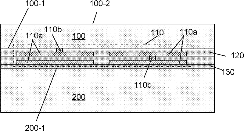
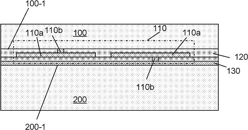
[0066] refer to figure 1 , figure 2 , is an embodiment of the substrate structure in which the bonding layer is an insulating layer and a conductive layer in this embodiment. As shown in the figure, the substrate structure includes:

[0067] The first substrate 100 and the second substrate 200 arranged oppositely;

[0068] The first surface 100-1 of the first substrate 100 faces the second surface 200-1 of the second substrate 200, and the first surface 100-1 is sequentially provided with a conductor interconnection layer 110 and a bonding layer 130;

[0069] The bonding layer 130 connects the first substrate 100 and the conductor interconnection layer 110 with the second substrate 200 .

[0070] Among them, such as figure 1 As shown, the bonding layer 130 may be an insulating layer, and may be a non-conductive material, such as silicon oxide, silicon oxynitride, or undoped amorphous silicon, or other suitable materials. In the embodiment where the bonding layer 130 is an...

Embodiment 2

[0093] The following will only describe the aspects that the second embodiment differs from the first embodiment. The parts not described should be considered to be performed by the same steps, methods or processes as those in Embodiment 1, and thus will not be repeated here.

[0094] refer to Figure 7 , Figure 8 , is an embodiment of the substrate structure in which the bonding layer is an insulating layer and a conductive layer in the second embodiment, and may further include an isolation region penetrating the first substrate on the basis of the substrate structure of the first embodiment, as shown in FIG. As shown, specifically, the substrate structure includes:

[0095] The first substrate 100 and the second substrate 200 arranged oppositely;

[0096] Through the isolation region 140 of the first substrate 100, the plurality of isolation regions 140 separate the first substrate 100 into mutually insulated regions;

[0097] The first surface 100-1 of the first subst...

Embodiment 3

[0110] The following will only describe the aspects that the third embodiment differs from the first embodiment. The parts not described should be considered to be performed by the same steps, methods or processes as those in Embodiment 1, and thus will not be repeated here.

[0111] Figure 9 , Figure 10 It is an embodiment of the substrate structure in which the bonding layer is an insulating layer and a conductive layer in Embodiment 3. On the basis of the substrate structure in Embodiment 1 or Embodiment 2, it may further include the first substrate in the second substrate The cavity 150 or the second cavity 152 between the first surface 100 - 1 and the second surface 200 - 1 , or further includes a combination of the first cavity 150 and the second cavity 152 .

[0112] like Figure 9 As shown, specifically, in some embodiments, the substrate structure includes:

[0113] The first substrate 100 and the second substrate 200 arranged oppositely;

[0114] The first sur...


PUM


Abstract

The invention provides a substrate structure, comprising a first substrate and a second substrate in opposite arrangement, wherein a first surface of the first substrate faces to a second surface of the second substrate; the first surface is provided with a conductor interconnection layer and a bonding layer in sequence; and the bonding layer is used for connecting the first substrate and the conductor interconnection layer with the second substrate. According to the substrate structure and the manufacturing method thereof, the second substrate is taken as a substrate with a supporting function; the first substrate is taken as a substrate for manufacturing a device directly; and the first substrate is formed by crystal growth, so the problems of thickness and self-stress are avoided, thus avoiding the unnecessary stress, thereby improving the performances of the devices formed in the first substrate.

Description

technical field [0001] The invention relates to the technical field of semiconductors, in particular to a substrate structure and a manufacturing method thereof. Background technique [0002] With the continuous development of integrated circuit technology, it has also been widely used in MEMS (Micro Electromechanical System, micro-electromechanical system), power devices and circuits, etc., by combining micro-mechanical technology or other technologies with integrated circuit manufacturing processes , Fabricate micro devices, micro systems or power devices, power circuits, etc. on the substrate of semiconductor materials. [0003] Traditionally, monocrystalline silicon substrates and SOI (Silicon On Insulator, silicon-on-insulator) substrates are mostly used for fabrication of devices. [0004] For SOI substrates, the price of SOI itself is high, and the manufacturing process of micromechanical devices and circuits is more complicated than traditional processes, which will...

Claims


Application Information

Patent Timeline
Patent Type & Authority Applications(China)
IPC IPC(8): H01L29/06H01L21/02H01L21/20
CPCH01L21/84H01L21/76283H01L21/76898H01L2924/0002H01L23/544H01L2223/54426H01L25/50B81C1/00182B81C1/00365B81C2201/019H01L2924/00H01L21/30H01L23/5226H01L23/528H01L23/562
Inventor 柳连俊
Owner MEMSEN ELECTRONICS
Learn More