Avalanche photodiode for ultraviolet detection as well as manufacturing method and working procedure thereof

An avalanche photoelectric and diode technology, applied in circuits, electrical components, semiconductor devices, etc., to achieve the effects of improving stability, saving manufacturing costs, and being easy to implement

Inactive Publication Date: 2011-11-09
JIANGSU CORENERGY SEMICON CO LTD
View PDF1 Cites 13 Cited by
  • Summary
  • Abstract
  • Description
  • Claims
  • Application Information

AI Technical Summary

Problems solved by technology

[0009] The problem to be solved by the present invention is: the existing wide-bandgap semiconductor PIN structure avalanche ultraviolet photodiode faces difficulties including complex preparation proc

Method used


Image

  • Avalanche photodiode for ultraviolet detection as well as manufacturing method and working procedure thereof
  • Avalanche photodiode for ultraviolet detection as well as manufacturing method and working procedure thereof
  • Avalanche photodiode for ultraviolet detection as well as manufacturing method and working procedure thereof

Examples


preparation example Construction

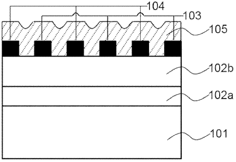
[0042] The preparation method of the above-mentioned metal-semiconductor-metal MSM planar structure wide bandgap semiconductor ultraviolet avalanche photodiode comprises the following steps:

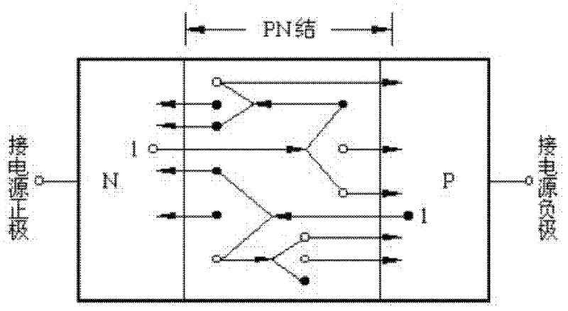
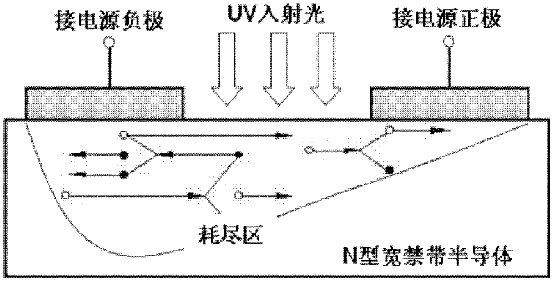
[0043] 1) Epitaxially grow the epitaxial layer of the epitaxially grown ultraviolet avalanche photodiode wafer on the homogeneous or heterogeneous substrate, the epitaxial layer structure includes buffer layer 102a, wide bandgap semiconductor light absorption layer 102b on the substrate from bottom to top, wide The bandgap semiconductor light-absorbing layer 102b can be a single-layer film or a multilayer film, and its basic feature is that the wide-bandgap semiconductor light-absorbing layer 102b has a bandgap width greater than 2.5eV, and a carrier concentration of less than 1×10 18 cm -3 The wide bandgap semiconductor material has a thickness between 50nm and 1mm. Typical wide bandgap semiconductors include GaN, AlN, ZnO, SiC, diamond, and ternary or quaternary alloy materials thereo...


PUM

PropertyMeasurementUnit
Bandgap widthaaaaaaaaaa
Carrier concentrationaaaaaaaaaa
Thicknessaaaaaaaaaa

Abstract

The invention provides an avalanche photodiode for ultraviolet detection as well as a manufacturing method and working procedure thereof. The avalanche photodiode comprises a substrate, a buffer layer, a light adsorption layer of a wide bandgap semiconductor and at least one pair of Schottky electrodes, wherein the buffer layer and the light adsorption layer of the wide bandgap semiconductor are arranged on the substrate in sequence; and the one pair of Schottky electrodes is horizontally distributed in a back-to-back mode and directly covers on the light adsorption layer of the wide bandgap semiconductor. Aiming at the problems that the quality of wide bandgap semiconductor crystals is generally low and a dual-conductive type doping is difficult to realize, a Schottky junction with high back bias voltage is utilized to realize an ultraviolet sensitive depletion region with a strong electric field; when the electric field in the depletion region reaches a critical breakdown field of the corresponding wide bandgap semiconductor, an avalanche operation can be realized; besides, a horizontal back-to-back Schottky contact structure is adopted so that the strong field in the semiconductor depletion region can be approximately perpendicular to the epitaxial growth direction of a semiconductor thin film, thus the influence of a structural defect in the material on device performances can be reduced and the reliability of a device can be improved.

Description

technical field [0001] The invention belongs to the technical field of semiconductor optoelectronic devices, and relates to an avalanche photodiode for ultraviolet detection, in particular to an avalanche photodiode for ultraviolet detection and a preparation method and working method thereof. Background technique [0002] Ultraviolet detection technology is a new type of photoelectric detection technology developed after infrared and laser detection technology. Due to its important applications in military and civilian use, ultraviolet detection technology has been given priority for development by major countries in the world for many years. At present, ultraviolet detectors are mainly divided into two categories: vacuum detectors and solid-state detectors. Vacuum detection devices are mainly based on ultraviolet photomultiplier tubes. Although ultraviolet photomultiplier tubes have been developed for many years and have been practically applied to ultraviolet early warn...

Claims


Application Information

Patent Timeline
IPC IPC(8): H01L31/0224H01L31/107H01L31/18
Inventor 陆海谢峰乔德瑞朱廷刚
Owner JIANGSU CORENERGY SEMICON CO LTD
Why Eureka
Try Eureka