Flat and lug combined bidirectional diode chip and manufacturing process thereof

A bidirectional diode and manufacturing process technology, which is applied in semiconductor/solid-state device manufacturing, electrical components, circuits, etc., can solve the problems that the chip performance is difficult to achieve the desired effect, the amount of acid used is uncontrollable, and the environment is damaged. It is not easy to break , reduced fragmentation rate, and wide adaptability

Active Publication Date: 2011-11-16
CHONGQING PINGWEI ENTERPRISE
View PDF6 Cites 10 Cited by
  • Summary
  • Abstract
  • Description
  • Claims
  • Application Information

AI Technical Summary

Problems solved by technology

[0002] At present, the production process of bidirectional diode chips (DB3-DB6) includes pickling process and GPP glass passivation process. The main problem of pickling process is that the amount of acid used is uncontrollable, the amount is large, and the damage to the environment is relatively large.
However, the cost of the GPP process is high, the corrosion depth is about 60 microns (um), the fragmentation rate is relatively high, and the controllability of the entire process is relatively poor; the performance of the chip produced by the above process is difficult to achieve the desired effect, and the damage resistance is weak

Method used


Image

  • Flat and lug combined bidirectional diode chip and manufacturing process thereof
  • Flat and lug combined bidirectional diode chip and manufacturing process thereof
  • Flat and lug combined bidirectional diode chip and manufacturing process thereof

Examples


Embodiment Construction

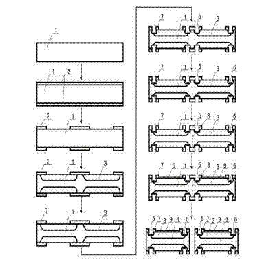
[0030] Below in conjunction with accompanying drawing, the present invention is described in further detail:

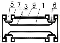
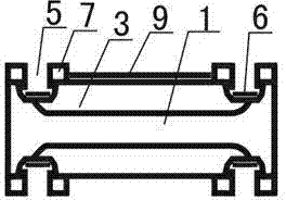
[0031] Such as figure 1 As shown, the flat and platform combined bidirectional diode chip of the present invention is processed from a P-type original silicon chip 1, and both sides of the chip are provided with a primary oxide layer near both ends (, figure 1 not visible in, see figure 2 In the primary oxide layer 2), the two sides of the chip are also provided with a phosphorus diffusion layer 3, and a secondary oxide layer is also provided on the primary oxide layer and the phosphorus diffusion layer 3. The secondary oxide layer and the primary oxide layer form an overlapping oxide layer 7. A mesa groove 5 is opened in the area where the oxide layer 7 overlaps, and a silicon nitride passivation layer 6 is arranged on the mesa groove 5, and nickel layers 9 are also arranged on the surface layers on both sides of the chip.

[0032] Such as figure 2 As shown, the...


PUM


Abstract

The invention discloses a flat and lug combined bidirectional diode chip which is processed by a P-type primary wafer; primary oxidization layers are arranged at positions, close to both ends, on two faces of a chip; the two faces of the chip are provided with phosphorous diffusion layers; secondary oxidization layers are arranged on the primary oxidization layers and the phosphorous diffusion layers; lug slots are formed in overlapped regions between the secondary oxidization layers and the primary oxidization layers; silicon nitride passivation layers are arranged on the lug slots; and the surfaces of the two faces of the chip are provided with nickel layers. The invention also discloses a manufacturing process for the flat and lug combined bidirectional diode chip. The manufacturing process comprises the following steps of: oxidizing for the first time, photoetching, diffusing phosphorous, oxidizing for the second time, photoetching the lug slots, passivating, photoetching lead wire holes, electroplating nickel and cutting to obtain the independent chip. The invention has the advantages that: as the mechanical intensity of the wafer and the wafer is hard to smash, the scribing (or cutting) efficiency is improved greatly; and compared with the scribing (or cutting) efficiency in a glass passivation process (GPP), the scribing (or cutting) efficiency is improved by over 40 percent, so the area of the whole graph can be saved by about 20 percent.

Description

technical field [0001] The invention relates to a bidirectional diode chip and a manufacturing process, in particular to a platform-platform combined bidirectional diode chip and a manufacturing process, belonging to the field of diode chip processing. Background technique [0002] At present, bidirectional diode chips (DB3-DB6) are produced by pickling process and GPP glass passivation process. The main problem of pickling process is that the amount of acid used is uncontrollable, the amount is large, and the damage to the environment is relatively large. However, the cost of the GPP process is high, the corrosion depth is about 60 microns (um), the fragmentation rate is relatively high, and the controllability of the entire process is relatively poor; the performance of the chip produced by the above process is difficult to achieve the desired effect, and the damage resistance is weak. Contents of the invention [0003] The object of the present invention is to provide a...

Claims


Application Information

Patent Timeline
Patent Type & Authority Applications(China)
IPC IPC(8): H01L29/861H01L29/06H01L21/329H01L21/78
Inventor 王兴龙邹红兵
Owner CHONGQING PINGWEI ENTERPRISE
Why Eureka
Try Eureka