
Sequential controllable nanometer silicon quantum dot array resistive random access memory and preparation method thereof

A technology of resistive memory and silicon quantum dots, which is applied in nanostructure manufacturing, nanotechnology, nanotechnology, etc., can solve the problem that silicon nanodot films cannot be used as resistive memory based on an ordered and controllable nano-silicon quantum dot array structure, etc. problems, to achieve high current densities

Active Publication Date: 2011-11-16
NANJING UNIV
View PDF4 Cites 14 Cited by
  • Summary
  • Abstract
  • Description
  • Claims
  • Application Information

AI Technical Summary

Problems solved by technology

The silicon nano-dot film prepared by this method cannot be used as a resistive memory based on an ordered and controllable nano-silicon quantum dot array structure.

Method used


Image

  • Sequential controllable nanometer silicon quantum dot array resistive random access memory and preparation method thereof
  • Sequential controllable nanometer silicon quantum dot array resistive random access memory and preparation method thereof
  • Sequential controllable nanometer silicon quantum dot array resistive random access memory and preparation method thereof

Examples


Embodiment 2

[0050] The difference between this embodiment and the above-mentioned embodiment lies in the decomposition of silane (SiH) on the P+ silicon substrate material. 4 ) And laughing gas (NO 2 ), so the amorphous hydrogen-containing silicon-rich silicon oxide (a-Si x O:H) Thin film sublayer instead of silicon nitride thin film sublayer. The ordered thyristor quantum dot array resistive memory thus obtained includes a P+ silicon substrate material, a resistive silicon quantum dot multilayer film nanopillar array attached to the substrate material, and a resistive silicon The upper and lower electrodes on the upper surface of the quantum dot multilayer film nanopillar array and the lower surface of the substrate; the resistive multilayer film nanopillar array has an insulating dielectric layer; the silicon quantum dot multilayer film nanopillar consists of at least 7-10 cycles It is composed of sublayers of silicon-rich silicon oxide films with different oxygen components embedded wit...


PUM

PropertyMeasurementUnit
heightaaaaaaaaaa
diameteraaaaaaaaaa

Abstract

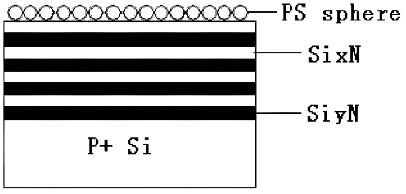
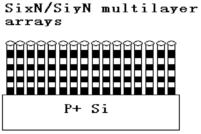
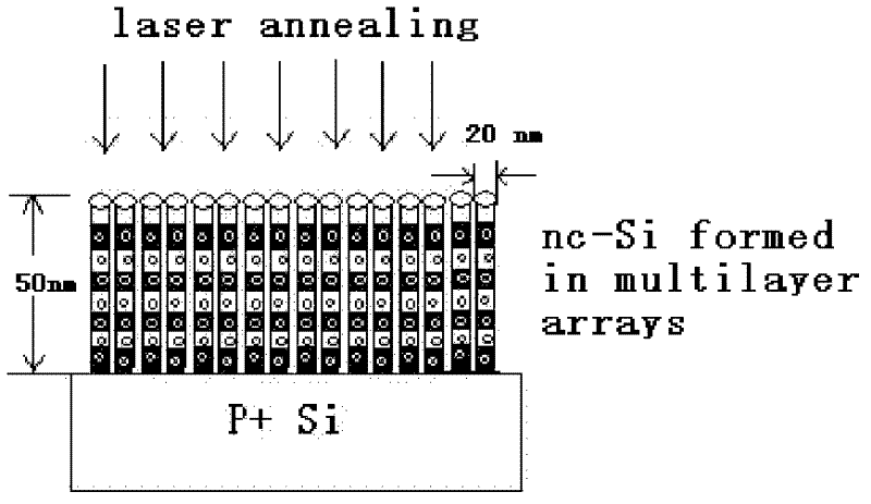
The invention relates to a sequential controllable nanometer silicon quantum dot array resistive random access memory and a preparation method thereof, and belongs to the technical field of non-volatile memories. The resistive random access memory comprises P and a silicon substrate material, and is characterized by also comprising a resistive silicon quantum dot multilayer film nanometer column array attached to the substrate material and an upper electrode and a lower electrode which are attached to the upper surface of the resistive silicon quantum dot multilayer film nanometer column array and the lower surface of the substrate; an insulating medium layer is arranged in the resistive multilayer film nanometer column array; and a silicon quantum dot multilayer film nanometer column is formed by at least two layers of silicon-enriched silicon nitride films which are inlaid with nanometer silicon quantum dots and have different nitrogen components or a silicon-enriched silicon oxide film sublayer which is inlaid with the nanometer silicon quantum dots and has different oxygen components. The sequential controllable nanometer silicon quantum dot array resistive random access memory can be compatible with the current micro-electronic process technology, and can show the advantage of sequential controllable nanometer silicon in resistive random access memory materials to fulfillthe aim of improving the switch ratio and stability of the resistive materials, so that nanometer silicon quantum dots are applied in silica-based nanometer memories in future.

Description

Technical field [0001] The invention involves a kind of blocking memory, especially an orderly controlled nano -silicon quantum dot matrix blocking memory, and also involves its preparation method, which is a non -volatile memory technology field. Background technique [0002] According to the applicant's understanding, in the past few decades, the vigorous development of electronic science and technology has brought the world into an information society, which has greatly changed human lifestyle and thinking models.The key device that supports information technology including information processing, transmission, and storage is high -density information memory. It is not only one of the main indicators of the development level of the national electronics technology, but also an important industry in the electronics industry. [0003] In recent years, various new types of next -generation non -volatile storage have emerged, such as iron -electric memory [1], magnetic memory (MRAM...

Claims


Application Information

Patent Timeline
Patent Type & Authority Applications(China)
IPC IPC(8): H01L45/00H01L27/28B82B3/00
Inventor 马忠元陈坤基徐岭夏国银江小帆杨华峰徐骏黄信凡冯端
Owner NANJING UNIV
Learn More