Manufacturing method of SU-8 photoresist micro-force sensor

A micro force sensor, SU-8 technology, applied in the field of micro sensors, can solve the problems of high cost, long production process cycle, and difficult control of silicon doping concentration, etc., and achieve low processing cost, good biocompatibility, small elastic mode volume effect

Inactive Publication Date: 2011-11-23
DALIAN UNIV OF TECH
View PDF4 Cites 7 Cited by
  • Summary
  • Abstract
  • Description
  • Claims
  • Application Information

AI Technical Summary

Problems solved by technology

[0003] At present, piezoresistive micro force sensors based on MEMS technology are mainly completed by silicon doping technology. T.Chu Duc and others from Delft University of Technology in the Netherlands have made a semiconductor silicon doping technology that can measure two Directional force micro force sensor (T Chu Duc, J F Creemer, and P M Sarro. Lateral nano-Newton force-sensing piezoresistive cantilever for microparticle handling. IOP science, 2006: 102-106.), but the doping concentration of silicon is not easy to control , and the production process cycle is relatively long, the cost is high

Method used


Image

  • Manufacturing method of SU-8 photoresist micro-force sensor
  • Manufacturing method of SU-8 photoresist micro-force sensor
  • Manufacturing method of SU-8 photoresist micro-force sensor

Examples


Embodiment Construction

[0022] specific implementation plan

[0023] The specific embodiments of the present invention will be described in detail below in conjunction with the technical solutions and accompanying drawings.

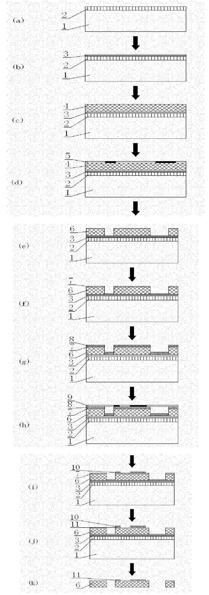
[0024] Such as figure 1 As shown in (a), after the silicon wafer 1 is cleaned by a standard cleaning solution, it is placed in an oxidation furnace to raise the temperature, and dry oxygen and wet oxygen are introduced in a certain order, so that a layer of dense silicon dioxide is formed on the surface of the silicon wafer. Layer 2, as the substrate. Such as figure 1 As shown in (b), a layer of Omnicoat adhesive layer 3 is spin-coated. By controlling the speed and time of the glue spinner, the thickness reaches about 1um, and then placed on a hot plate at 120°C for 30 minutes. Such as figure 1 As shown in (c), spin-coat a layer of SU-8 adhesive layer 4, by controlling the speed and time of the glue spinner, make its thickness reach about 25um, after standing for a period of...


PUM


Abstract

The invention discloses a manufacturing method of a SU-8 photoresist micro-force sensor, wherein the SU-8 photoresist micro-force sensor is a microsensor belonging to the technical field of microelectromechanical systems. The manufacturing method is characterized by adopting silicon as a substrate material and omnicoat as a bonding layer material and a sacrificial layer material, and comprising the following steps of carrying out a first exposure and development process to obtain a SU-8 photoresist structure, carrying out a sputtering process, carrying out a second exposure and development process to obtain a positive photoresist mask, carrying out a metal layer corrosion process, and carrying out a releasing process. A sensor manufactured through the manufacturing method can be connected to a peripheral circuit through two electrodes to form a Wheatstone bridge and can convert resistance variations into voltage variations thereby measuring an acting force. A photoresist adopted by the manufacturing method is a SU-8 photoresist and the SU-8 photoresist has low modulus of elasticity, thus performances of a SU-8 photoresist micro-force sensor manufactured by the manufacturing method are similar to that of a semiconductor silicon micro-force sensor and the SU-8 photoresist micro-force sensor has good biological compatibility. The manufacturing method has the advantages of simple process, low cost, short processing cycle and good feasibility for volume production.

Description

technical field [0001] The invention belongs to micro-sensors in the technical field of micro-electro-mechanical systems, and relates to a manufacturing method of SU-8 glue micro-force sensors. Background technique [0002] The main processing technology of the MEMS sensor follows the semiconductor manufacturing process. In addition to the commonly used silicon material, its base material also includes quartz, GaAs polymer and metal materials. What's more, because the core of the MEMS sensor - the sensitive element or has moving parts or needs to be in contact with the working medium, this leads to some design and packaging are more complex compared with traditional microelectronics. The cost of MEMS sensor packaging process and test calibration accounts for more than 80% of the total product cost. Due to the diversity and particularity of its packaging forms, it also makes the standardization of MEMS sensors more difficult. As an important sensor in MEMS, micro-force senso...

Claims


Application Information

Patent Timeline
Patent Type & Authority Applications(China)
IPC IPC(8): B81C1/00
Inventor 褚金奎陈兆鹏张然
Owner DALIAN UNIV OF TECH
Why Eureka
Try Eureka