Graphene graphing methods

A patterning, graphene technology, applied in electrical components, semiconductor/solid-state device manufacturing, circuits, etc., can solve the problems of unavailability, graphene pollution, and difficult process, and achieve the effect of low cost

Active Publication Date: 2011-11-30
SHANGHAI INST OF MICROSYSTEM & INFORMATION TECH CHINESE ACAD OF SCI
View PDF5 Cites 18 Cited by
  • Summary
  • Abstract
  • Description
  • Claims
  • Application Information

AI Technical Summary

Problems solved by technology

Based on the preparation of micro-nano devices, graphene usually needs to be patterned. At present, the commonly used graphene patterning methods include: 1) performing photolithography and ion etching processes on the transferred large-area graphene to obtain patterned graphite Graphene, this method has high patterning accuracy, but the process is difficult, and it is easy to cause pollution and damage to graphene during

Method used


Image

  • Graphene graphing methods
  • Graphene graphing methods
  • Graphene graphing methods

Examples


Embodiment 1

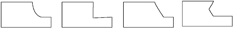
[0032] Square patterning graphene

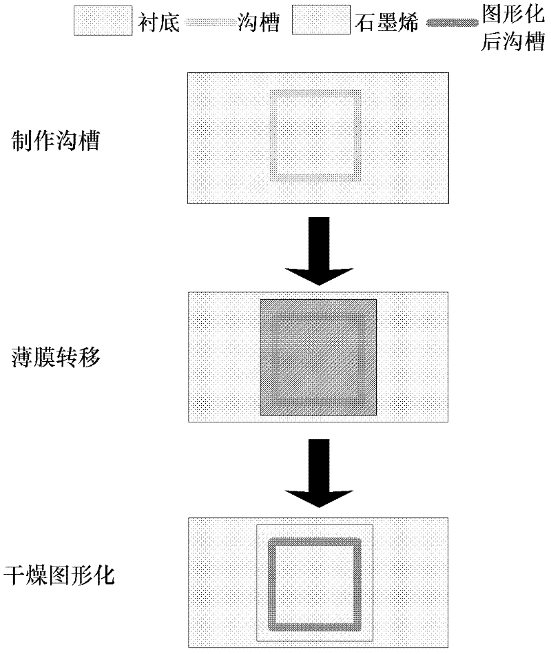
[0033] 1. Directly use micro-cutting technology to cut a 5×5mm square groove on the ceramic substrate. The groove boundary width is 30um and the depth is 40um. The groove pattern and the top view of the substrate are as follows Figure 4 shown;

[0034] 2. The graphene obtained by mechanical exfoliation is transferred to acetone;

[0035] 3. Take the graphene film directly from the substrate with the pattern in acetone, and the film covers the pattern;

[0036] 4. After drying at 200°C for 15 minutes, patterned graphene can be obtained at the substrate pattern.

Embodiment 2

[0038] Fabrication of composite patterned graphene films

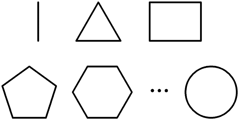
[0039] 1. Photolithography plate and substrate patterns such as Figure 5 As shown, the pattern is a combination of rectangle (0.5×3mm) and square (2×2mm), with a border width of 20um. The silicon substrate is spin-coated with 5um thick glue, then photolithography, developed and then dried, using deep reactive ion etching. Etch a trench of 30um on the silicon substrate, remove glue, clean and dry after etching;

[0040] 2. Large-area high-quality graphene prepared by CVD method on Cu foil was transferred to deionized water;

[0041] 3. Use the trench substrate to fish the graphene film in the solution, and the film covers the trench;

[0042] 4. After drying at 40°C for 30 minutes, patterned graphene can be obtained at the substrate pattern, and then metal devices can be made on the square area to make striped graphene devices (such as Figure 5 shown).

Embodiment 3

[0044] Fabrication of graphene with six-electrode polygons

[0045] 1. Make a trench substrate, the photolithographic pattern is as follows Figure 6 Shown, technological process is identical with the technological process in step 1 among the embodiment 2;

[0046] 2. Steps 2, 3, and 4 are the same as steps 2, 3, and 4 in Example 2.

[0047] The method for patterning graphene provided by the invention is mainly characterized in that:

[0048] 1. Use the method of deep reactive ion etching, micro-cutting technology or wet etching in the micro-technology processing process to produce the required groove pattern on the substrate. The pattern can be linear, circular, rectangular, polygonal, or comb-shaped. etc. and combinations thereof;

[0049] 2. The substrate can be silicon wafer, silicon oxide wafer, ceramics, glass, etc.;

[0050] 3. The graphic boundary is a groove with a certain width and depth, and the aspect ratio is > 1.1;

[0051] 3. Different trench etching method...


PUM


Abstract

The invention discloses a method for graphic modeling of graphene by using grooves which are formed on a substrate, comprising the following steps: manufacturing a graph structure taking the grooves as boundaries on the substrate by using a DRIE (deep reactive ion etching) technology, a micro cutting technology or a wet etching technology in a micromachining technology; transferring a supportlesslarge-area graphene film to the graphic modeling substrate with the grooves from a solution; and drying the substrate and the graphene, and breaking the graphene in a groove area by using the surfacetension of the solution so as to obtain the required graphic modeling graphene. By the method, the position of the graphic modeling graphene can be accurately determined on the substrate in no need of carrying out photoetching on the graphene, thus preventing the crystal lattice quality of the graphene from being damaged and solving the problems that the cost is high, the positioning is difficultand the pollution occurs easily in the former graphene graphical modeling process.

Description

technical field [0001] The invention relates to the technical field of semiconductor devices, in particular to a patterning method capable of precisely positioning graphene. Background technique [0002] Graphene is a material formed by a single layer of carbon atoms arranged into a two-dimensional regular hexagonal honeycomb lattice, which maintains a nearly perfect crystal structure and high stability, and exhibits such as room temperature quantum Hall effect, ballistic transport, A series of novel physical properties such as massless Dirac fermions. Since graphene won the Nobel Prize in Physics in 2010, graphene has aroused widespread research upsurge. [0003] At present, graphene has been proved to be applicable to the preparation of various electronic devices, such as molecular sensors, field effect transistors, solar cells and so on. Based on the preparation of micro-nano devices, graphene usually needs to be patterned. At present, the commonly used graphene pattern...

Claims


Application Information

Patent Timeline
IPC IPC(8): H01L21/02
Inventor 李铁王文荣王跃林
Owner SHANGHAI INST OF MICROSYSTEM & INFORMATION TECH CHINESE ACAD OF SCI
Why Eureka
Try Eureka