Preparation methods for arrayed nickel silicon nanowire and nickel silicon-silicon core-shell nanowire

A nanowire, nickel-silicon technology, applied in the field of material science, can solve the problems of harsh reaction conditions, inability to achieve arrayed structure growth, and cumbersome reaction process, and achieve the effect of excellent performance.

Active Publication Date: 2011-11-30
ZHEJIANG UNIV
View PDF1 Cites 10 Cited by
  • Summary
  • Abstract
  • Description
  • Claims
  • Application Information

AI Technical Summary

Problems solved by technology

However, these methods still face some problems, such as the inability to grow high-density arrayed structures on large substrates, cumbersome reaction process, harsh reaction conditions, and poor conductivity of electrodes, etc.

Method used


Image

  • Preparation methods for arrayed nickel silicon nanowire and nickel silicon-silicon core-shell nanowire
  • Preparation methods for arrayed nickel silicon nanowire and nickel silicon-silicon core-shell nanowire
  • Preparation methods for arrayed nickel silicon nanowire and nickel silicon-silicon core-shell nanowire

Examples


Embodiment 1

[0031] (1) Foam nickel is cleaned respectively with dilute hydrochloric acid and alcohol, then with vacuum drying or nitrogen blow-drying for subsequent use; The mass percentage concentration of dilute hydrochloric acid is 10%, and the volume percentage concentration of alcohol is 98%;

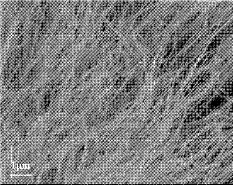
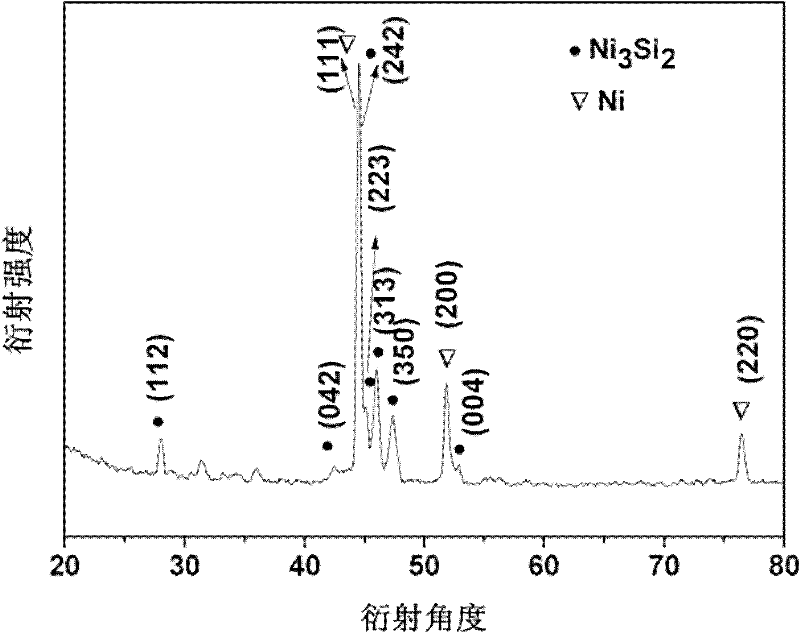
[0032] (2) Place the cleaned foam nickel in the hot wire chemical vapor deposition device, set the silane flow to 80sccm, the hydrogen flow to 80sccm, the chamber pressure to 600Pa, the temperature to be 500°C, and the reaction time to be 15min. Arrayed nickel-silicon nanowires are grown on the surface of nickel foam;

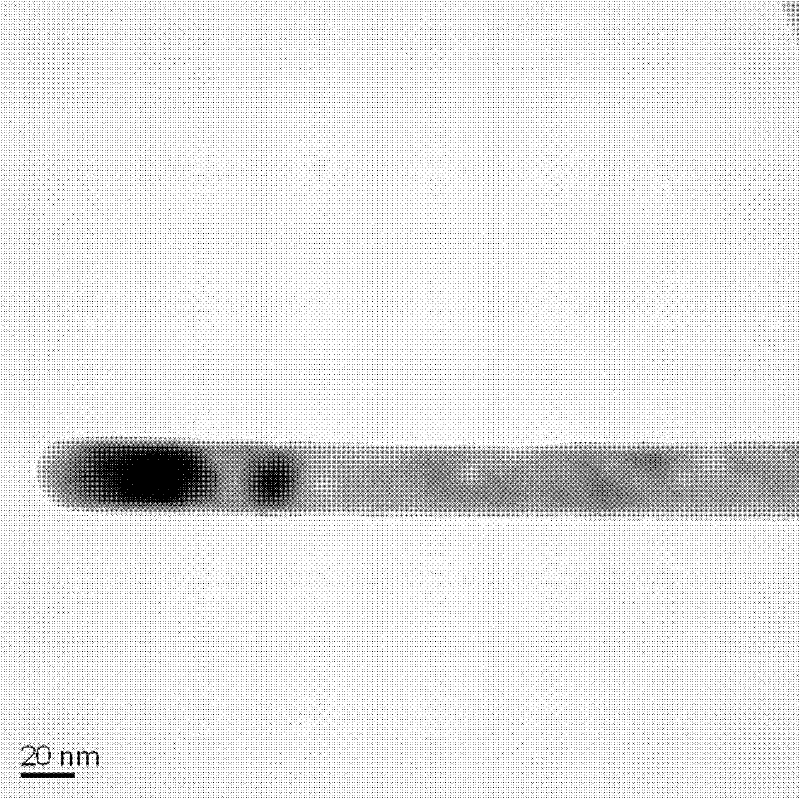
[0033] (3) Deposit a layer of silicon with controllable thickness on the surface of the arrayed nickel-silicon nanowires obtained in step (2) by radio frequency sputtering. The temperature of the silicon substrate is set to 20° C., and the argon flow is 30 sccm. The gas pressure is 3Pa, the sputtering power is 80W, and the sputtering time is 60min, and arrayed nickel-silicon-si...

Embodiment 2

[0039](1) Nickel foil is cleaned separately with dilute hydrochloric acid and alcohol, then with vacuum drying or nitrogen blow-drying standby; The mass percent concentration of dilute hydrochloric acid is 5%, and the volume percent concentration of alcohol is 90%;

[0040] (2) Place the cleaned foamed nickel in the hot wire chemical vapor deposition device, set the silane flow rate to 10 sccm, the hydrogen flow rate to 10 sccm, the chamber air pressure to 10 Pa, the temperature to 200 ° C, and the reaction time to be 1 min. Arrayed nickel-silicon nanowires are grown on the surface of nickel foam;

[0041] (3) Deposit a layer of silicon with a controllable thickness on the surface of the arrayed nickel-silicon nanowires by radio frequency sputtering. The power is 10W, and the sputtering time is 1min, and arrayed nickel-silicon-silicon core-shell nanowires are obtained.

[0042] The test results are similar to Example 1.

Embodiment 3

[0044] (1) The foamed copper plated with nickel on the surface is cleaned separately with dilute hydrochloric acid and alcohol, and subsequently dried with vacuum or nitrogen for subsequent use; the mass percent concentration of dilute hydrochloric acid is 20%, and the volume percent concentration of alcohol is 80%;

[0045] (2) Place the cleaned foamed nickel in the hot wire chemical vapor deposition device, set the silane flow rate to 100sccm, the hydrogen flow rate to 1000sccm, the chamber pressure to 1000Pa, the temperature to 400°C, and the reaction time to be 30min. Arrayed nickel-silicon nanowires are grown on the surface of nickel foam;

[0046] (3) A layer of silicon with controllable thickness is deposited on the surface of the arrayed nickel-silicon nanowires by radio frequency sputtering. The power is 50W, the sputtering time is 30min, and arrayed nickel-silicon-silicon core-shell nanowires are obtained.

[0047] The test results are similar to Example 1.


PUM

PropertyMeasurementUnit
diameteraaaaaaaaaa
thicknessaaaaaaaaaa

Abstract

The invention discloses preparation methods for an arrayed nickel silicon nanowire and a nickel silicon-silicon core-shell nanowire. The preparation method for the nickel silicon-silicon core-shell nanowire comprises the following steps of: washing a metal substrate for a lithium ion battery anode basal body by using a hydrochloric acid and ethanol, and drying the washed metal substrate for lateruse; growing the arrayed nickel silicon nanowire on the surface of the washed metal substrate by using a hot wire chemical vapor deposition device; and further depositing a layer of thickness-controllable silicon on the surface of the obtained arrayed nickel silicon nanowire by using a radio frequency sputtering method to obtain the arrayed nickel silicon-silicon core-shell nanowire. The metal substrate and the arrayed nickel silicon nanowire grown on the metal substrate form a lithium ion battery anode. The preparation methods provided by the invention are simple and controllable; and the prepared nanowire materials can be used for the lithium ion battery anode and high performance can be obtained.

Description

technical field [0001] The invention belongs to the field of material science, and in particular relates to a method for preparing arrayed nickel-silicon nanowires and nickel-silicon-silicon core-shell nanowires used for negative electrodes of lithium-ion batteries. Background technique [0002] Due to its relatively high theoretical capacity, silicon is considered to be an ideal substitute for lithium-ion battery anode graphite-like carbon materials, thereby meeting the needs of high-energy-density lithium-ion batteries. However, due to the huge volume change during the charging and discharging process, it will lead to the pulverization of the silicon electrode material, and its capacity will drop sharply; in addition, the performance of the silicon electrode material is unstable under a large charging and discharging current, which limits its use as a lithium battery. Commercial application of ion battery anode materials. [0003] At present, more and more work is devoted...

Claims


Application Information

Patent Timeline
Patent Type & Authority Applications(China)
IPC IPC(8): H01M4/1395B82Y40/00
CPCY02E60/12Y02E60/122Y02E60/10
Inventor 杜宁樊星吴平杨德仁
Owner ZHEJIANG UNIV
Why Eureka
Try Eureka