Preparation methods for arrayed nickel silicon nanowire and nickel silicon-silicon core-shell nanowire
A nanowire, nickel-silicon technology, applied in the field of material science, can solve the problems of harsh reaction conditions, poor electrode conductivity, cumbersome reaction process, etc., and achieve the effect of excellent performance
- Summary
- Abstract
- Description
- Claims
- Application Information
AI Technical Summary
Problems solved by technology
Method used
Image
Examples
Embodiment 1
[0031] (1) Foam nickel is cleaned respectively with dilute hydrochloric acid and alcohol, then with vacuum drying or nitrogen blow-drying for subsequent use; The mass percentage concentration of dilute hydrochloric acid is 10%, and the volume percentage concentration of alcohol is 98%;
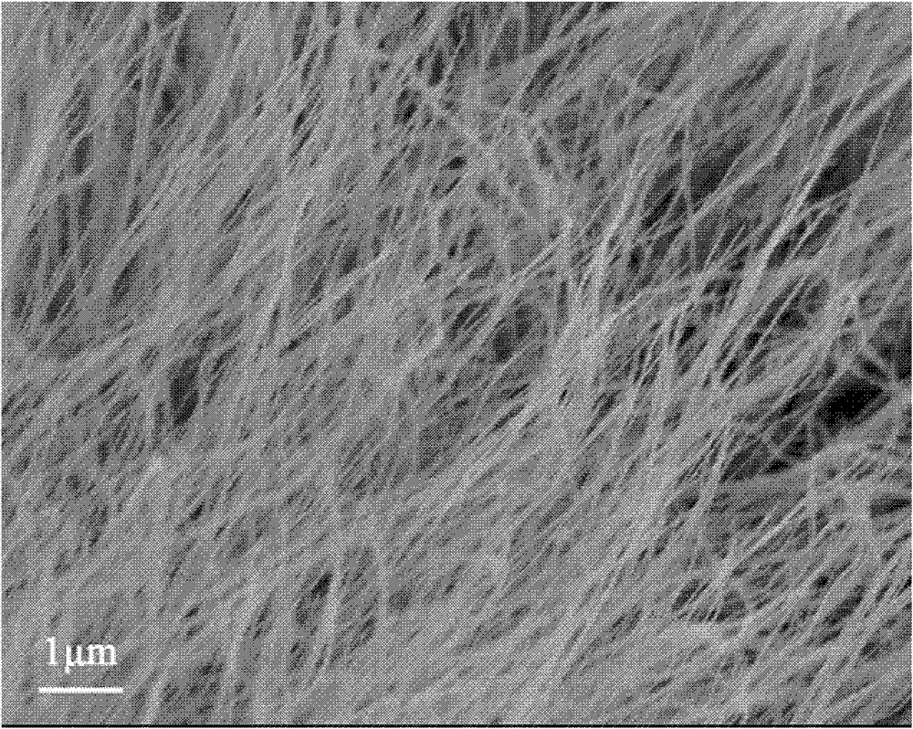
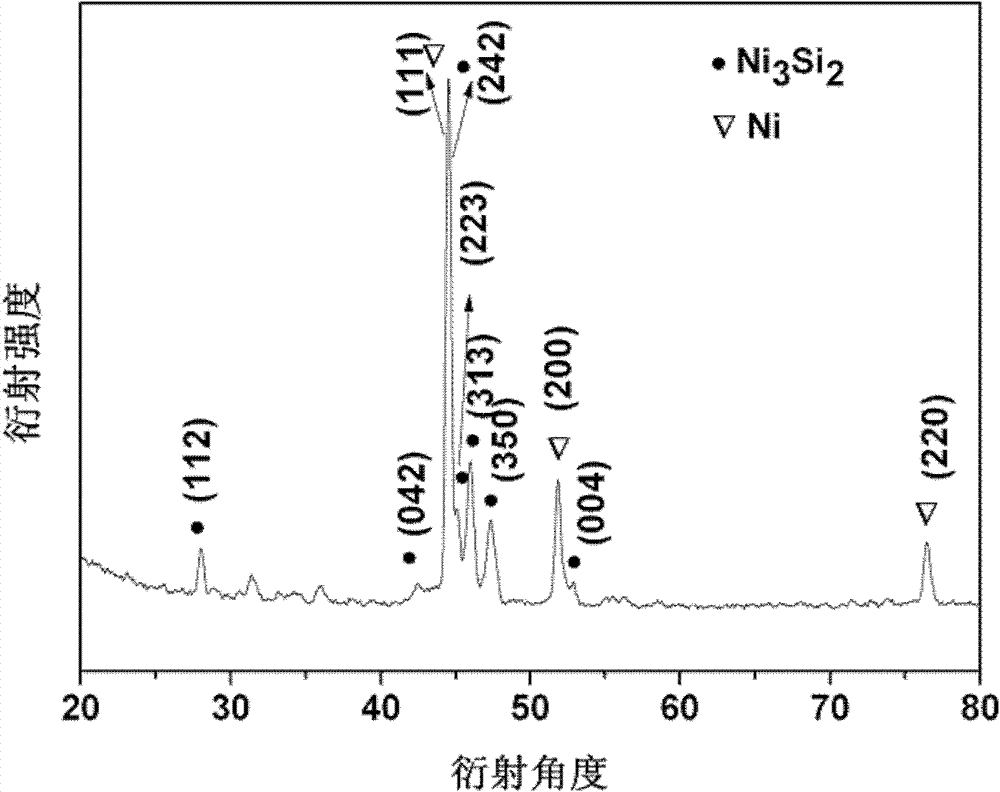
[0032] (2) Place the cleaned foam nickel in the hot wire chemical vapor deposition device, set the silane flow to 80sccm, the hydrogen flow to 80sccm, the chamber pressure to 600Pa, the temperature to be 500°C, and the reaction time to be 15min. Arrayed nickel-silicon nanowires are grown on the surface of nickel foam;
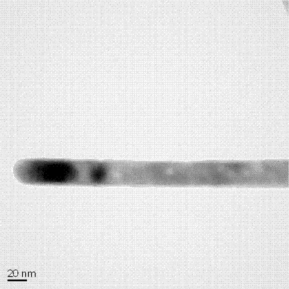
[0033] (3) Deposit a layer of silicon with controllable thickness on the surface of the arrayed nickel-silicon nanowires obtained in step (2) by radio frequency sputtering. The temperature of the silicon substrate is set to 20° C., and the argon flow is 30 sccm. The gas pressure is 3Pa, the sputtering power is 80W, and the sputtering time is 60min, and arrayed nickel-silicon-si...
Embodiment 2
[0039](1) Nickel foil is cleaned separately with dilute hydrochloric acid and alcohol, then with vacuum drying or nitrogen blow-drying standby; The mass percent concentration of dilute hydrochloric acid is 5%, and the volume percent concentration of alcohol is 90%;
[0040] (2) Place the cleaned foamed nickel in the hot wire chemical vapor deposition device, set the silane flow rate to 10 sccm, the hydrogen flow rate to 10 sccm, the chamber air pressure to 10 Pa, the temperature to 200 ° C, and the reaction time to be 1 min. Arrayed nickel-silicon nanowires are grown on the surface of nickel foam;
[0041] (3) Deposit a layer of silicon with a controllable thickness on the surface of the arrayed nickel-silicon nanowires by radio frequency sputtering. The power is 10W, and the sputtering time is 1min, and arrayed nickel-silicon-silicon core-shell nanowires are obtained.
[0042] The test results are similar to Example 1.
Embodiment 3
[0044] (1) The foamed copper plated with nickel on the surface is cleaned separately with dilute hydrochloric acid and alcohol, and subsequently dried with vacuum or nitrogen for subsequent use; the mass percent concentration of dilute hydrochloric acid is 20%, and the volume percent concentration of alcohol is 80%;
[0045] (2) Place the cleaned foamed nickel in the hot wire chemical vapor deposition device, set the silane flow rate to 100sccm, the hydrogen flow rate to 1000sccm, the chamber pressure to 1000Pa, the temperature to 400°C, and the reaction time to be 30min. Arrayed nickel-silicon nanowires are grown on the surface of nickel foam;
[0046] (3) A layer of silicon with controllable thickness is deposited on the surface of the arrayed nickel-silicon nanowires by radio frequency sputtering. The power is 50W, the sputtering time is 30min, and arrayed nickel-silicon-silicon core-shell nanowires are obtained.
[0047] The test results are similar to Example 1.
PUM
| Property | Measurement | Unit |
|---|---|---|
| diameter | aaaaa | aaaaa |
| thickness | aaaaa | aaaaa |
Abstract
Description
Claims
Application Information


