Systems, methods and substrates for single crystal germanium crystal growth

A technology for crystal growth and single crystal germanium, which is applied in the directions of single crystal growth, single crystal growth, crystal growth, etc., and can solve the problems of limitation and unusability of arsenic doping methods

Inactive Publication Date: 2011-12-07
AXT INC +1
View PDF2 Cites 8 Cited by
  • Summary
  • Abstract
  • Description
  • Claims
  • Application Information

AI Technical Summary

Problems solved by technology

However, for VGF and VB technologies where the crucible is encapsulated in ampoules, the method described cannot be used
In addition, the special requirements for the growth of specially doped germanium single crystals

Method used


Image

  • Systems, methods and substrates for single crystal germanium crystal growth
  • Systems, methods and substrates for single crystal germanium crystal growth
  • Systems, methods and substrates for single crystal germanium crystal growth

Examples


Embodiment Construction

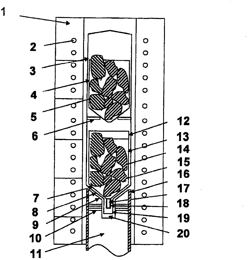
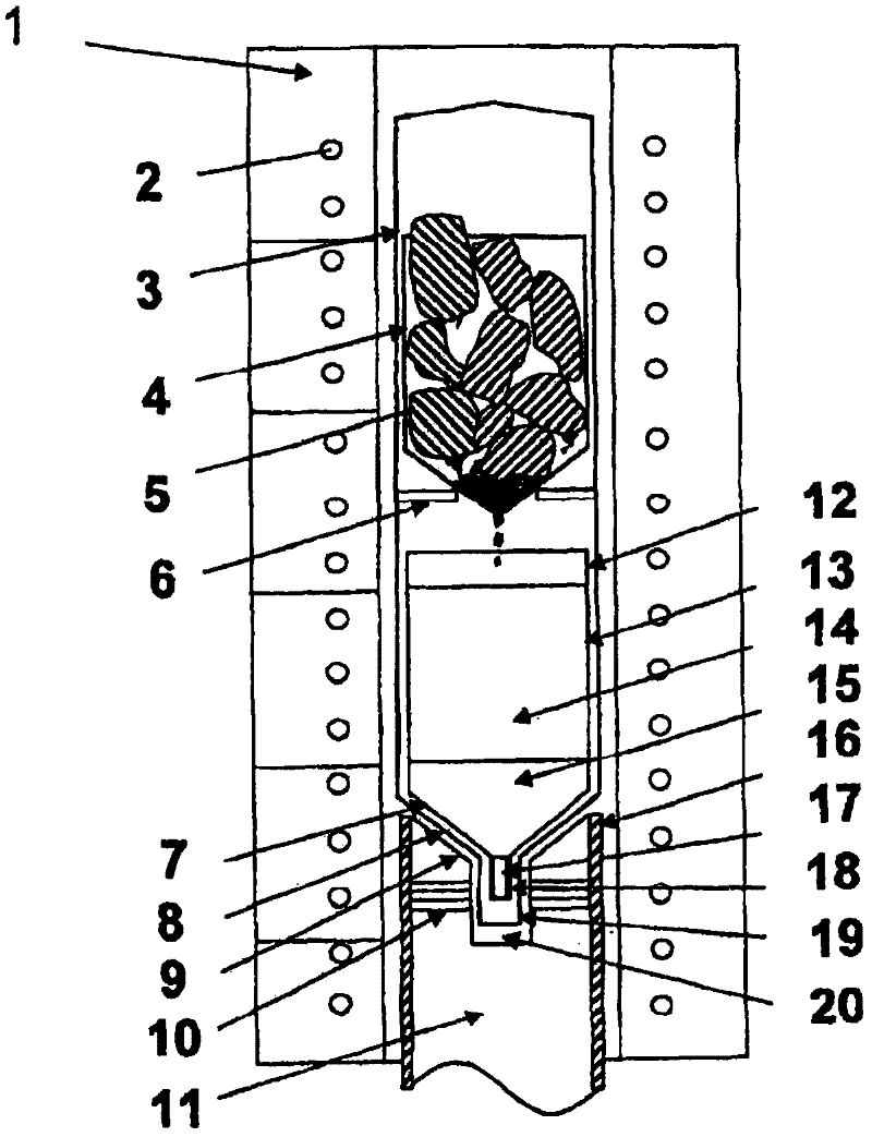
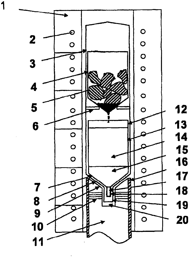
[0018] The invention will now be described in detail, examples of which are illustrated in the accompanying drawings. The embodiments given in the following specification do not represent all embodiments consistent with the claimed invention. Rather, they are merely some examples consistent with certain aspects of the invention. Wherever possible, the same reference numbers will be used throughout the drawings to refer to the same or like parts.

[0019] Aspects of the present invention are particularly suited for the apparatus and methods for growing germanium ingot crystals having a diameter of 150 mm (6 inches), which are described herein. However, it should be understood that some aspects of the present invention have greater utility, such as the use of related apparatus and methods to produce germanium (Ge) ingots with diameters greater than 50 mm (2 inches), such as diameters of 100 mm (4 inches) and 200mm (8 inches) boule.

[0020] and Figure 1A-Figure 2 Consistent...


PUM


Abstract

Systems, methods, and substrates for growth of single crystal germanium (Ge) are disclosed. In an exemplary embodiment, a method of growing a single crystal germanium (Ge) crystal is provided. Additionally, the method may comprise charging the first Ge feedstock into a crucible, charging the second Ge feedstock into a container for replenishing the Ge melt material, sealing the crucible and container within the ampoule, Putting the ampoule with the crucible into a crystal growth furnace, and melting the first Ge raw material and the second Ge raw material, and controlling the crystallization temperature gradient of the melt to reproducibly provide single crystal germanium crystals with improved/desired properties ingot.

Description

[0001] Cross-reference of related application information [0002] This application is based upon and claims the benefit / priority of prior Chinese Patent Application No. 200810177006.0, filed November 10, 2008, and U.S. Patent Application No. 12 / 544,902, filed September 5, 2009, of which The entire contents are incorporated herein by reference. technical field [0003] The present invention relates to the growth of single crystal germanium (Ge) crystals and related systems, methods and substrates. Background technique [0004] Manufacturers of electrical and optoelectronic devices generally require large semiconductor single crystals with uniform electrical properties, which are used as substrates for the production of microelectric devices after slicing and polishing. The growth of semiconductor crystals involves heating polycrystalline feedstock to its melting point (typically in excess of 1,200°C) to create a polycrystalline feedstock melt, contacting the melt with high...

Claims


Application Information

Patent Timeline
IPC IPC(8): C30B29/08C30B15/20
Inventor 刘卫国
Owner AXT INC
Why Eureka
Try Eureka