High-speed electrically regulated terahertz modulator

A terahertz, electrical control technology, applied in instruments, nonlinear optics, optics, etc., can solve the problems of low modulation speed, difficult to achieve steep band gap edge of THz modulator, modulation depth and insertion loss are not very ideal, etc. Effects of high-speed modulation

Active Publication Date: 2011-12-14
SUZHOU INST OF NANO TECH & NANO BIONICS CHINESE ACEDEMY OF SCI
View PDF7 Cites 29 Cited by
  • Summary
  • Abstract
  • Description
  • Claims
  • Application Information

AI Technical Summary

Problems solved by technology

In recent years, people have developed bandgap shifting THz modulators based on THz waves of artificial electromagnetic materials such as photonic crystals and metamaterials. The modulation depth can reach 30dB and the modulation speed is about 10kHz. However, these THz The bandgap edge of the modulator is difficult to achieve steepness, and indicators such as modulation depth and insertion loss are not very ideal
The THz modulator based on the artificial structure of Metamaterials is also a research hotspot at present, but the modulation speed of such devices is still low, and the performance index is difficult to improve
In fact, at present, the modulation speed of THz modulators through electrical control is only a few hundred Hz to kHz, which is difficult to meet the requirements of THz applications in the field of communication and imaging. key

Method used


Image

  • High-speed electrically regulated terahertz modulator
  • High-speed electrically regulated terahertz modulator
  • High-speed electrically regulated terahertz modulator

Examples


preparation example Construction

[0033] The preparation, testing and analysis process of the high-speed electrical modulation terahertz modulator is as follows:

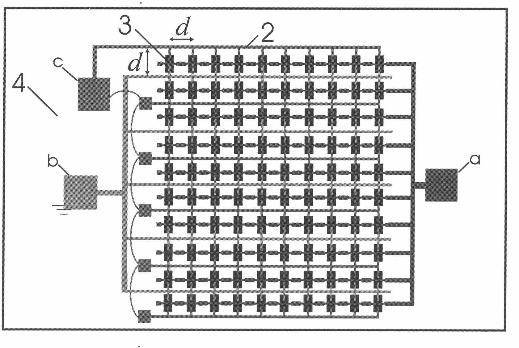
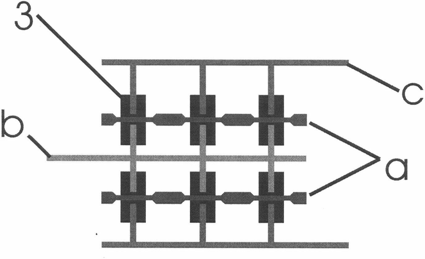
[0034] Step 1: Using the software FDTD Solution based on the finite difference in time domain, establish the model structure of the terahertz wave modulator, in which the metallic frequency selective surface structure 2 is set to 200 nanometers thick gold. By optimizing the gate G, source S, and drain D dimensions, the simulation obtains the maximum relative modulation depth when the channel conductance is turned on and off in a gated high electron mobility transistor. The best parameters obtained are: source width S=1 micron, drain width D=1 micron and gate width G=7 micron, periodic unit spacing d=50 micron, modulator relative modulation depth in frequency range 0.82-0.92THz 75%.

[0035] Step 2: Prepare a photolithography plate, use the inductively coupled plasma etching method to etch the transistor substrate mesa, and use the photoresist as a ...


PUM


Abstract

The invention discloses a high-speed electrically-modulating terahertz modulator. The high-speed electrically-modulating terahertz modulator comprises a medium substrate (4), wherein the medium substrate (4) is made of a material which is transparent to terahertz waves; an array which is formed by high electron mobility transistors (3) is distributed on the surface of the medium substrate (4); a frequency selecting surface structure (2) is attached to the surface of the medium substrate and the surface of the array of the high electron mobility transistors, and is a graphical conductive film with a bandpass filtering structure; the source electrode (b), the drain electrode (c) and the grid electrode (a) of each high electron mobility transistor are formed on the part of the conductive film, which corresponds to each high electron mobility transistor; and the electron mobility of the high electron mobility transistors is more than 1,500cm<2> / Vs. A high-speed modulation effect on the amplitude of the terahertz waves is achieved by the high-speed electrically-modulating terahertz modulator in an electrically modulating mode, a modulating speed can be more than 10MHz, and a relative modulating depth is over 50 percent.

Description

technical field [0001] The invention particularly relates to a device capable of high-speed and high-efficiency modulation of the terahertz wave amplitude through an electrical control method, which can be applied to the fields of terahertz communication, terahertz imaging and the like. Background technique [0002] Terahertz (THz) waves are electromagnetic waves with frequencies ranging from 0.1THz to 10THz, and wavelengths ranging from 30μm to 3mm, between millimeters and infrared. Compared with electromagnetic waves in other bands, THz waves have low photon energy and penetrating Excellent properties such as strong strength have great scientific research value and broad market prospects in basic research fields such as physics, chemistry and medical science, as well as applied research fields such as safety inspection, environmental monitoring, and communication. With the rapid development of THz technology, the gap in the THz gap is gradually being filled, and semiconduc...

Claims


Application Information

Patent Timeline
Patent Type & Authority Applications(China)
IPC IPC(8): G02F1/015
Inventor 张晓渝秦华吴东岷李欣幸张宝顺
Owner SUZHOU INST OF NANO TECH & NANO BIONICS CHINESE ACEDEMY OF SCI
Why Eureka
Try Eureka