A testing device for a phase-change memory cell array

A unit array and testing device technology, applied in the field of micro-nano electronics, achieves the effects of simple structure, flexible operation, and accurate electrical characteristic parameters

Active Publication Date: 2011-12-21
HUAZHONG UNIV OF SCI & TECH
View PDF3 Cites 26 Cited by
  • Summary
  • Abstract
  • Description
  • Claims
  • Application Information

AI Technical Summary

Problems solved by technology

Therefore this method cannot be used to test if Image 6 The phase-change memory storage unit integrated with the CMOS circuit shown, this structure is called 1T1R structure

Method used


Image

  • A testing device for a phase-change memory cell array
  • A testing device for a phase-change memory cell array
  • A testing device for a phase-change memory cell array

Examples


Embodiment 1

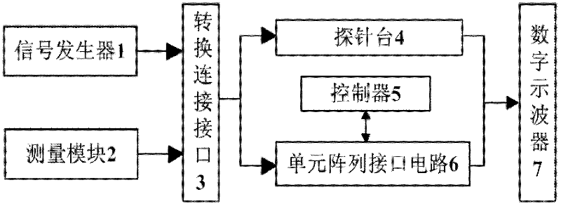
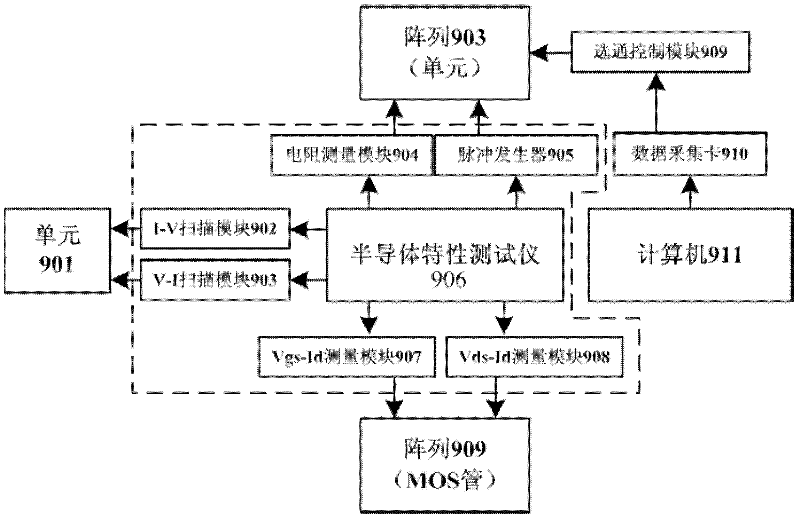
[0035] figure 2 An example of a phase-change memory cell array testing device, the signal generator 1 adopts a pulse signal generator 905, and the measurement module 2 adopts an I-V scanning module 902, a V-I scanning module 903, and a resistance measurement module 904 integrated in a semiconductor characteristic tester 909 , Vgs-Id measurement module 907, Vds-Id measurement module 908, wherein I-V scanning module 902, V-I scanning module 903 are used for the test of unit 901, resistance measurement module 904, pulse generator 905 are used for the unit test in the array, Vgs -Id measurement module 907, Vds-Id measurement module 908 is used for the test of the MOS tube in the array; The conversion connection interface adopts the integrated source and measurement unit SMU integrated in the semiconductor characteristic tester; the probe station 4 connects the unit to be tested 901 into the test device, the unit array interface circuit 6 connects the array 909 or 903 to be tested...

Embodiment 2

[0055] The unit under test adopts such as Figure 7 The phase-change memory unit shown, the thickness of each layer of film is: the lower electrode TiW film 100nm; the second layer of SiO 2 Thin film 150nm; third layer GST thin film 100nm; fourth layer SiO 2 The thin film is 150nm; the upper electrode TiW thin film is 150nm.

[0056] Initial resistance test. Use the DC voltage scanning function of the semiconductor characteristic tester to scan the unit from 0V to 0.2V with a step size of 0.1V, and the measured resistance is 283.7K ohms, indicating that the unit is conductive and in an amorphous state.

[0057] Initialize the unit. After applying a single pulse with a height of 1.5V and a width of 150ns to the cell, the measured resistance is 16K ohms, indicating that the cell has been initialized to a crystalline state.

[0058] Test unit DC I-V characteristics. Apply a write pulse excitation to the unit, the amplitude is 4.6V, the pulse width is 50ns, the falling edge i...

Embodiment 3

[0061] Select an array of 1T1R structure with a MOS tube width-to-length ratio of 50u:500n, and use the cell array interface circuit 6 to respectively lead out the source, drain and gate of the MOS tubes. Connect the SMU of the Keithley 4200 semiconductor characteristic tester to the gate and drain of the MOS transistor, and the source and substrate of the MOS transistor to ground. Set it to MOS tube module test in the semiconductor characteristic tester, and the test steps are as follows:

[0062] Test the Vgs-Id curve. A sweep voltage of 0-3 V was applied on the gate while the current on the drain was measured. The obtained scanning result curve shows that the MOS tube can work normally, and the threshold voltage is 0.8V.

[0063] Test the Vds-Id curve. The gate is given from 0V to 3V at every 0.5V step, and the drain is scanned from 0-3.3V with a step of 0.05V. The graph of the scanning result shows that the MOS tube can work normally.


PUM


Abstract

The invention discloses a device for testing a phase change memory unit. The device comprises a signal generator, a measuring module, a conversion connection interface, a probe station, a controller, a unit array interface circuit and a digital oscilloscope, wherein a control signal is applied through the controller; an excitation signal is applied through the signal generator; and direct current I-V characteristics, pulse I-V characteristics, threshold voltage, threshold current, the minimum write pulse amplitude, the minimum write pulse width, the minimum erasing pulse amplitude, the minimum erasing pulse width, data retention time, erasing fatigue testing and other electrical characteristics of the phase change memory unit are tested by acquiring signals through the measuring module or the oscilloscope. By the device, the direct current I-V characteristics, the pulse I-V characteristics, the threshold voltage, the threshold current, amorphous resistance, crystalline resistance, the minimum write pulse amplitude, the minimum write pulse width, the minimum erasing pulse amplitude, the minimum erasing pulse width, the data retention time, the erasing fatigue testing and other electrical characteristics of the phase change memory unit can be accurately measured.

Description

technical field [0001] The invention belongs to the technical field of micro-nano electronics, and in particular relates to an electrical performance testing device of a phase-change memory cell array. Background technique [0002] Phase change memory uses chalcogenide compounds as the storage medium, and uses electric energy to convert the material between crystalline (low resistance) and amorphous (high resistance) to realize data writing and erasing, so that the phase change memory unit is changed from crystal to The pulse that changes from the amorphous state to the amorphous state is called a wipe pulse, and the pulse that changes from an amorphous state to a crystalline state is called a write pulse; data readout is achieved by measuring the change in resistance. Therefore, it belongs to resistive non-volatile memory. [0003] Since phase-change memory was proposed in the late 1960s, due to the limitation of semiconductor process technology, the development of phase-c...

Claims


Application Information

Patent Timeline
Patent Type & Authority Applications(China)
IPC IPC(8): G11C29/56
Inventor 缪向水瞿力文张乐彭菊红李震
Owner HUAZHONG UNIV OF SCI & TECH
Why Eureka
Try Eureka