Manufacturing method of silicon epitaxial wafer for low voltage tvs

A manufacturing method and technology of silicon epitaxial wafers, applied in semiconductor/solid-state device manufacturing, electrical components, circuits, etc., can solve problems such as long-term reliability impact and damage of devices, and achieve the effect of ensuring protection voltage and reducing compensation degree

Active Publication Date: 2011-12-21
NANJING GUOSHENG ELECTRONICS
View PDF4 Cites 9 Cited by
  • Summary
  • Abstract
  • Description
  • Claims
  • Application Information

AI Technical Summary

Problems solved by technology

Therefore, ESD damage has become one of the main reliability problems of integrated circuits. Studies have shown that in most cases ESD damage is manifested as potential damage, so that the long-term reliability of the device is seriously affected. Therefore, the circuit must have a low clamping voltage. Protection devices with fast response time to ensure effective ESD protection

Method used


Image

  • Manufacturing method of silicon epitaxial wafer for low voltage tvs
  • Manufacturing method of silicon epitaxial wafer for low voltage tvs
  • Manufacturing method of silicon epitaxial wafer for low voltage tvs

Examples


Embodiment Construction

[0010] The present invention will be described in detail below in conjunction with the accompanying drawings and specific embodiments.

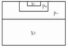
[0011] The low-voltage ESD protection device is the key device of the transient voltage suppressor (TVS), which adopts a new composite punch-through device structure (such as figure 1 ). First, a P-type high-resistance epitaxial layer is epitaxially grown on the N+ substrate, and a P+ well is formed on the epitaxial layer, and then an N+ region is formed on the well by diffusion, so that the depletion layer is depleted under reverse bias. Extend to N + substrate region, forming N + P + P - N + Four layers of structure. A thin base region width is formed through process control to reduce the breakdown voltage of the PN junction to meet the voltage requirements of low-voltage ESD devices. In addition, the lightly doped epitaxial layer P- can prevent reverse biased N + P + An avalanche breakdown occurs. Moreover, this structure is easy...


PUM


Abstract

The invention relates to a manufacturing method for a silicon epitaxial wafer, in particular to a manufacturing method for a silicon epitaxial wafer of a low-voltage TVS (transient voltage suppressor). In the technical scheme, when a P-shaped epitaxial layer is grown on an N-shaped substrate, HCl (Hydrogen Chloride) is adopted for gas corrosion of impurities and metal atoms on the surface of the substrate, high-temperature large-volume hydrogen is then adopts for blowing, hydrogen is adopted for high-temperature baking of impurity atoms on the N-shaped substrate, and finally a pre-pass P-typedopant (B2H6) is grown on the epitaxial layer. Therefore, the concentration of gas-phase impurities in an epitaxial reactor and the concentration of impurities absorbed to a base and the surface of the substrate can be reduced, the degree of compensation of N-type impurities and P-type impurities can be decreased, and a clean growth zone can be formed. Moreover, gas-phase conditions in the reactor can be improved, the stability of the thickness of the epitaxial layer can be guaranteed, and thus, the stability of protective voltage for devices can be ensured.

Description

technical field [0001] The invention relates to a silicon epitaxial wafer, in particular to a method for manufacturing a silicon epitaxial wafer for a low-voltage TVS, and belongs to the field of silicon epitaxial wafer manufacturing. Background technique [0002] With the continuous development of electronic communication technology, communication equipment with high density, miniaturization and complex functions has become the mainstream of the market. However, due to its low operating voltage, it is extremely vulnerable to the threat of electrostatic discharge (ESD), and even has destructive consequences. At the same time, due to the gradual shrinking of the feature size of devices, the feature size of IC products has reached the order of tens of nanometers, and the active layer and gate oxide layer of integrated circuits are relatively thinner, so they are more sensitive to instantaneous current and voltage shocks in the circuit. Therefore, ESD damage has become one of ...

Claims


Application Information

Patent Timeline
Patent Type & Authority Applications(China)
IPC IPC(8): H01L21/20H01L21/329
Inventor 马林宝金龙骆红
Owner NANJING GUOSHENG ELECTRONICS
Why Eureka
Try Eureka