

A kind of led device and led module device thereof
A technology for LED devices and LED modules, which is applied in the direction of electric solid state devices, semiconductor devices, electrical components, etc., can solve problems such as the reduction of light efficiency, and achieve the effect of high luminous efficiency and good heat dissipation performance.
- Summary
- Abstract
- Description
- Claims
- Application Information
AI Technical Summary
Problems solved by technology
Method used
Image

Examples
Embodiment 1
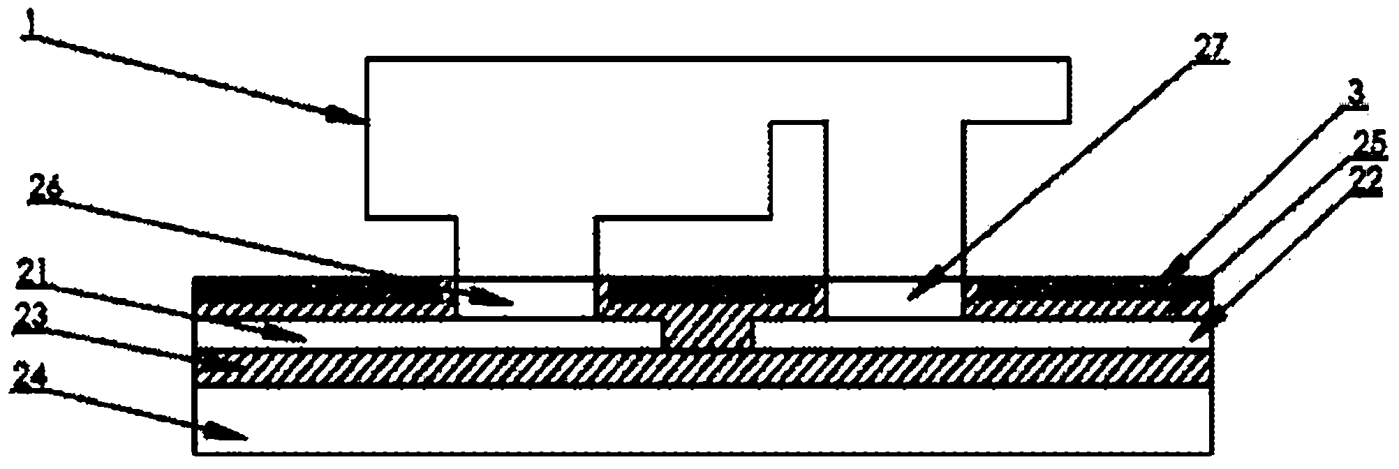
[0048] Such as figure 2 As shown, this embodiment discloses an LED device, including a plurality of LED chips 1 (only one LED chip is schematically shown in the figure), and a substrate 2, and the LED chip 1 shown is flip-chip on the substrate 2 .
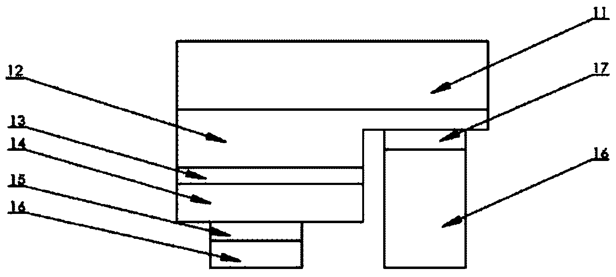
[0049] Such as figure 1 As mentioned above, the LED chip 1 includes a sapphire substrate 11 , an N-type gallium nitride 12 , a multi-layer quantum well light-emitting layer 13 , a P-type gallium nitride 14 , a P electrode 15 , a metal bump 16 and an N electrode 17 . N-type GaN 12 is grown on the sapphire substrate 11 , a light-emitting layer 13 is grown on the N-type GaN 12 , and a P-type GaN 14 is grown on the light-emitting layer 13 . Through process steps such as photolithography, etching, metal layer deposition and passivation layer protection, and finally through the split process, P electrodes 15 and metal bumps 16 are formed on the P-type GaN 14 layer, and on the N-type GaN 12 N electrodes 17 and metal bumps 16 are formed ...
Embodiment 2
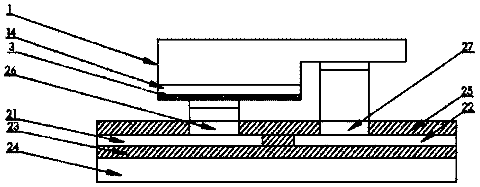
[0063] Such as image 3 As shown, the difference between this embodiment and embodiment 1 is that: the position of the high reflection layer 3 is disposed on the lower surface of the P-type gallium nitride 14 of the LED chip 1 .
[0064] In this embodiment, since the reflective layer 3 is disposed on the P-type gallium nitride layer 14, the thickness of the first heat dissipation layer 25 deposited on the metal electrode layer can be the same as the height of the P pad 26 and the N pad 27 on the substrate 2; Since the first heat dissipation layer adopts diamond-like carbon film (DLC) or diamond film, it has high heat dissipation, can accelerate the heat from the LED chip to circulate in the lateral direction, and quickly introduce heat to the metal substrate, and because the diamond-like carbon film ( DLC) or diamond film has excellent characteristics of hardness and wear resistance, and the diamond-like film (DLC) or diamond film deposited on the metal electrode layer plays a...
Embodiment 3
[0066] Such as Figure 4 Shown, the difference between this embodiment and embodiment 1 is:
[0067] (1) A diamond-like carbon film (DLC) or a diamond film is also attached to the side walls of the P pad 26 and the N pad 27 to further improve the heat dissipation effect of the LED device.
[0068] (2) The high reflective layer 3 is a multi-layer distributed Bragg reflective layer formed by the periodic growth of the following materials:
[0069] Indium (In), Aluminum (Al), Gold (Au), Platinum (Pt), Zinc (Zn), Silver (Ag), Titanium (Ti), Silicon Nitride (SiNx), Silicon Dioxide (SiO 2 ), aluminum oxide (Al 2 o 3 ), titanium monoxide (TiO), titanium dioxide (TiO 2 ), titanium dioxide (Ti 2 o 3 ), and zirconium dioxide (ZrO 2 ).
[0070] The Bragg reflection layer is a layered structure in which two materials with different refractive indices are grown alternately periodically, and can reflect the light incident on the substrate back to the upper surface by using the Bragg...
PUM
| Property | Measurement | Unit |
|---|---|---|
| Thickness | aaaaa | aaaaa |
Abstract
Description
Claims
Application Information