Silicon wafer degumming device

A silicon wafer and deionized water technology, applied in the processing of photosensitive materials, can solve the problems of underlying silicon loss, damage to the sensitive structure of the wafer surface, etc., and achieve minimum loss, low mean square error roughness, and high deglue efficiency Effect

Active Publication Date: 2013-03-06
无锡影速半导体科技有限公司
View PDF0 Cites 4 Cited by
  • Summary
  • Abstract
  • Description
  • Claims
  • Application Information

AI Technical Summary

Problems solved by technology

For the removal of implanted photoresist on silicon, alkaline or acidic fluorine-based solutions can be used, but it will cause loss of the underlying silicon; plasma removal technology can also be used, but the charge generated by the non-uniform plasma will damage the crystal. Sensitive structures on round surfaces

Method used


Image

  • Silicon wafer degumming device
  • Silicon wafer degumming device

Examples


Embodiment Construction

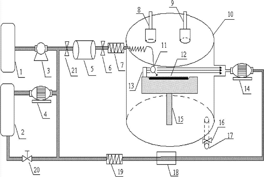
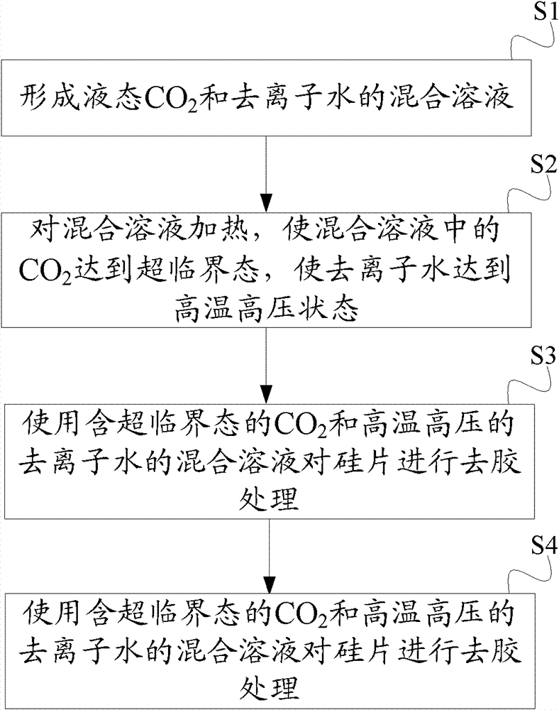
[0014] Such as figure 1 As shown, the silicon wafer degumming device provided by the embodiment of the present invention includes a deionized water storage tank 1, a CO 2 Gas storage tank 2, for deionized water and CO 2 5. Heating the mixed solution to make the CO in the mixed solution 2 A heat exchanger 7 that reaches a supercritical state and makes deionized water reach high temperature and high pressure, a reaction chamber 10 for removing glue from silicon wafers 12, CO 2 Recovery device. The reaction chamber 10 is provided with a rotatable tray 15 for placing a silicon wafer 12 coated with photoresist, a CO for stripping the stripped photoresist tape from the surface of the silicon wafer 12. 2 Source 13 (which may be a cylinder), temperature sensor 8 and pressure sensor 9 . CO 2 The source 13 is used to lift the stripped photoresist tape away from the surface of the sample sheet and be taken out of the reaction chamber 10 at the same time. The tray 15 containing the ...


PUM


Abstract

The invention discloses a silicon wafer degumming device, which comprises deionized water storage tank, a CO2 storage tank, a mixing tank, a heat exchanger and a reaction cavity, wherein the heat exchanger is used for heating a mixed solution, and the reaction cavity is used for degumming a silicon wafer; and an outlet of the deionized water storage tank and an outlet of the CO2 storage tank are connected with one end of a mixing tank, and the other end of the mixing tank is connected with an inlet of the reaction cavity through the heat exchanger. The invention also discloses a silicon wafer degumming method, which comprises the following steps of: heating the mixed solution so that CO2 in the mixed solution reaches a supercritical state and the deionized water reaches a high-temperature and high-pressure state; and degumming the silicon wafer by using the mixed solution containing the supercritical CO2 and the high-temperature and high-pressure deionized water. According to the device and method provided by the invention, organic photoresist on an inorganic carbonized thick layer and bottom are completely oxidized and dissolved, therefore the degumming efficiency is higher without residues, and the loss of film materials is minimized.

Description

technical field [0001] The invention relates to a semiconductor stripping technology / photoresist stripping technology, in particular to a silicon wafer stripping device and method. Background technique [0002] In the modern CMOS device manufacturing process, almost all substrate structures are formed by ion implantation. The energetic ions can damage the photoresist, making it difficult to remove. After implantation, these ions may exist as oxide layers, sub-oxide layers, or organic compounds. These energetic ions also transform the photoresist surface into a carbonaceous layer of diamond-type and graphite-type mixtures. The carbonization process therefore makes removal of implanted photoresist challenging. For the removal of implanted photoresist on silicon, alkaline or acidic fluorine-based solutions can be used, but it will cause loss of the underlying silicon; plasma removal technology can also be used, but the charge generated by the non-uniform plasma will damage t...

Claims


Application Information

Patent Timeline
Patent Type & Authority Patents(China)
IPC IPC(8): G03F7/42
Inventor 王磊景玉鹏
Owner 无锡影速半导体科技有限公司
Why Eureka
Try Eureka