Method for graphical film

A patterning and film layer technology, applied in the direction of electrical components, semiconductor/solid-state device manufacturing, circuits, etc., can solve problems such as unresolved

Inactive Publication Date: 2012-01-11
SHANGHAI HUAHONG GRACE SEMICON MFG CORP
View PDF4 Cites 7 Cited by
  • Summary
  • Abstract
  • Description
  • Claims
  • Application Information

AI Technical Summary

Problems solved by technology

[0004] In the prior art, there are many methods for patterning film layers using photoresist, such as the "Method for Forming Patterned Film Layers and Barrier Ribs" disclosed in Chinese Patent No. 1779571 published on May 31, 2006. , did not solve the above problems

Method used


Image

  • Method for graphical film
  • Method for graphical film
  • Method for graphical film

Examples


Embodiment Construction

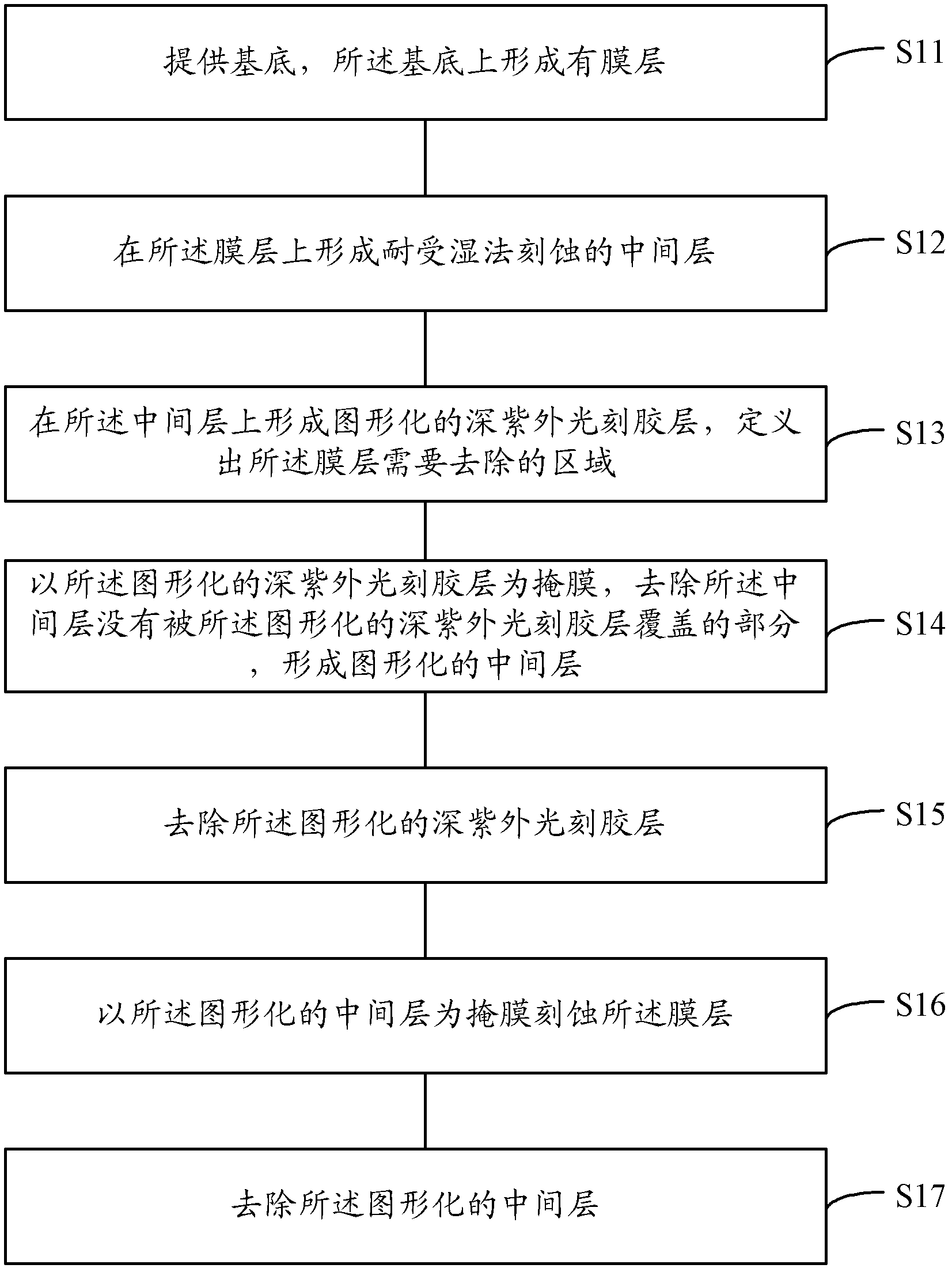
[0030] The method for patterning the film layer in the specific embodiment of the present invention combines the intermediate layer resistant to wet etching with the deep ultraviolet photoresist layer, and first transfers the pattern on the deep ultraviolet photoresist layer to the intermediate layer, so that the intermediate layer The line width of the layer is the same as that of the deep ultraviolet photoresist layer. After removing the deep ultraviolet intermediate layer, the patterned intermediate layer can be used as a mask to etch the film layer, so that the line width of the film layer is less than or equal to 350nm .

[0031] In order to make the above objects, features and advantages of the present invention more comprehensible, specific implementations of the present invention will be described in detail below in conjunction with the accompanying drawings.

[0032] In the following description, specific details are set forth in order to provide a thorough understand...


PUM


Abstract

The method relates to a method for a graphical film. The method comprises the following steps that: a substrate is provided, wherein a film is formed on the substrate; an intermediate layer is formed on the film; a graphical deep ultra-violet photoresist layer is formed on the intermediate layer and an area that is needed to be removed on the film is defined; the graphical deep ultra-violet photoresist layer is utilized as a mask to remove a portion of the intermediate layer, wherein the portion has not been covered by the graphical deep ultra-violet photoresist layer, so that a graphical intermediate layer is formed; the graphical deep ultra-violet photoresist layer is removed; the graphical intermediate layer is utilized as a mask to etch the film; and the graphical intermediate layer is removed. In the prior art, when a line width of a graph of a film is reduced to a certain size or a smaller size ( less than or equal to 350 millimeters), it is necessary to utilize a deep ultra-violet photoetching technology to manufacture a graph; and subsequent wet etching of the film do not allow the deep ultra-violet photoresist to be used as a mask; however, the above-mentioned problem is solved by the method provided in the invention.

Description

technical field [0001] The invention relates to the technical field of semiconductors, in particular to a method for patterning a film layer. Background technique [0002] With the development of semiconductor technology, in the process of forming a metal oxide semiconductor field effect transistor (MOSFET), in order to reduce the contact plug and the contact resistance between single crystal silicon and polycrystalline silicon, a metal silicide will be formed. A common method for forming a salicide is to react metals such as cobalt, nickel, and titanium with silicon. [0003] In the prior art, the process of forming metal silicide is: provide a silicon substrate, and form a layer of silicon oxide on the silicon substrate; then, form a photoresist layer on the silicon oxide; Perform exposure and development to form a pattern in the photoresist layer, which defines the pattern of the silicon oxide to be etched; after that, use the patterned photoresist as a mask to wet-etch ...

Claims


Application Information

Patent Timeline
Patent Type & Authority Applications(China)
IPC IPC(8): H01L21/027H01L21/768
Inventor 宗登刚徐爱斌于涛于世瑞孔蔚然
Owner SHANGHAI HUAHONG GRACE SEMICON MFG CORP
Why Eureka
Try Eureka