

Method for making micro nanometer structure device by laser two-photon direct writing technology
A micro-nano structure and two-photon technology, which is applied in the manufacture of micro-structure devices, micro-structure devices, micro-structure technology, etc., can solve the problems that cannot be directly applied to the manufacturing process of semiconductor devices, and achieve low cost, wide application prospects, and reduced process The effect of steps
- Summary
- Abstract
- Description
- Claims
- Application Information
AI Technical Summary
Problems solved by technology
Method used
Image

Examples
example 1
[0069] The following combination Figure 5-12 , the method of the present invention will be described in detail by taking the fabrication of a FinFET device on an SOI substrate as an example.
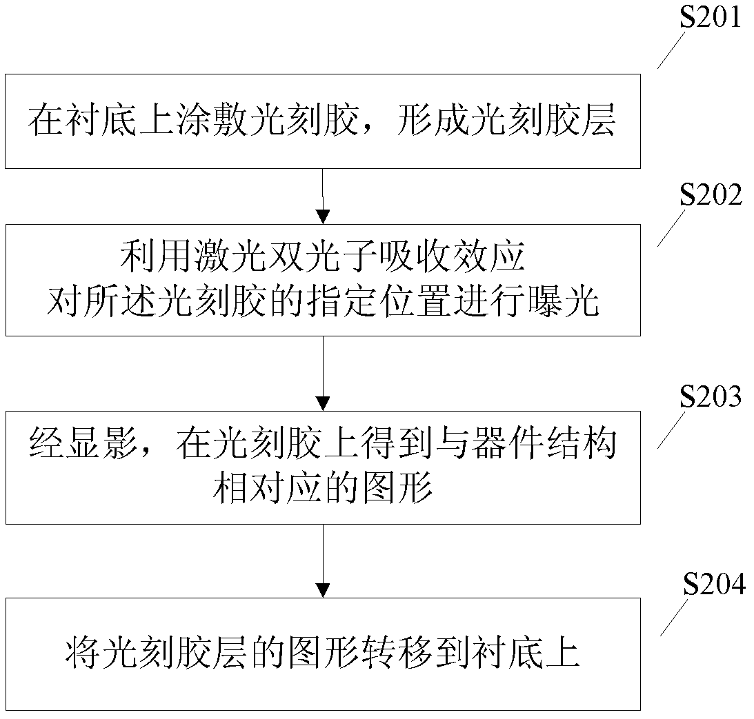
[0070] First, a photoresist is coated on the SOI substrate to form a photoresist layer.
[0071] A negative photoresist with trade name SCR500 is coated on the SOI substrate to obtain a photoresist layer 501, such as Figure 5 shown. The SOI substrate is composed of a top silicon layer 502 , a silicon oxide insulating layer 503 and a silicon substrate 504 from top to bottom. The thickness of the top silicon layer is, for example, 55 nm, and the thickness of the silicon oxide insulating layer is, for example, 150 nm.
[0072] Secondly, the photoresist layer is exposed by means of laser two-photon absorption, and the FinFET device pattern is exposed in the photoresist layer.
[0073] Turn on the laser light source in the laser micro-nanofabrication system. The laser source is a titan...
example 2
[0083] Referring to FIG. 13 , the method of the present invention will be described in detail by taking the preparation of a metal grid structure on a GaAs substrate as an example.
[0084] First, a layer of positive photoresist AZ4620 with a thickness of 180 nm is coated on the GaAs substrate 1301 to form a photoresist layer 1302, such as Figure 13A shown. The pre-baking temperature of the photoresist is, for example, 95° C., and the pre-baking time is 90 s.
[0085] Secondly, the positive photoresist is exposed by using laser two-photon absorption effect.
[0086] Adjust the laser light source in the laser micro-nano processing system, and adjust the output wavelength of the laser to a single wavelength that can cause the coated photoresist to produce a two-photon effect, that is, 780nm. Adjust the exposure time to 1ms-10min by adjusting the shutter on the laser light path. Adjust the optical attenuator of the laser light path to adjust the laser power to 0.1μW-1W. Adju...
example 3
[0093] The present invention will be described in detail below by taking the preparation of a two-dimensional metal lattice on a glass substrate as an example.
[0094] First, coat a layer of positive photoresist AZ6130 with a thickness of 120 nm on the glass substrate. The photoresist pre-baking temperature is 90°C, and the pre-baking time is 100s;
[0095] Second, the positive photoresist is exposed using the two-photon absorption effect of a single-wavelength laser beam. By adjusting the laser power to 1.99mW and the exposure time to 10ms to control the exposure conditions of the photoresist, a hole array with an aperture of 370nm can be formed, such as Figure 14A shown.
[0096] Further, using the photoresist formed with the hole array as a mask, an Au layer with a thickness of, for example, 60 nm is evaporated.
[0097] Further, the photoresist on the surface of the glass is peeled off, and the Au layer above the photoresist is peeled off at the same time to obtain a ...
PUM
| Property | Measurement | Unit |
|---|---|---|
| thickness | aaaaa | aaaaa |
| thickness | aaaaa | aaaaa |
| thickness | aaaaa | aaaaa |
Abstract
Description
Claims
Application Information