Manufacturing process of monocrystalline silicon ingot and thermal field structure of ingot furnace

A manufacturing process, monocrystalline silicon technology, applied in the field of crystal growth in the photovoltaic industry, can solve the problem that the conversion rate of polysilicon is only 15%~16%, achieve the effect of improving photoelectric conversion efficiency, increasing production, and improving economic benefits of enterprises

Inactive Publication Date: 2012-01-25
ZHEJIANG JINGGONG NEW ENERGY
View PDF3 Cites 13 Cited by
  • Summary
  • Abstract
  • Description
  • Claims
  • Application Information

AI Technical Summary

Problems solved by technology

[0004] The output of polysilicon single ingot has reached 550kg, and the largest ingot even reaches 1 ton. The cutting rate is around 57%~60%. The conversion rate is only 15%~16%

Method used


Image

  • Manufacturing process of monocrystalline silicon ingot and thermal field structure of ingot furnace
  • Manufacturing process of monocrystalline silicon ingot and thermal field structure of ingot furnace
  • Manufacturing process of monocrystalline silicon ingot and thermal field structure of ingot furnace

Examples


specific Embodiment approach

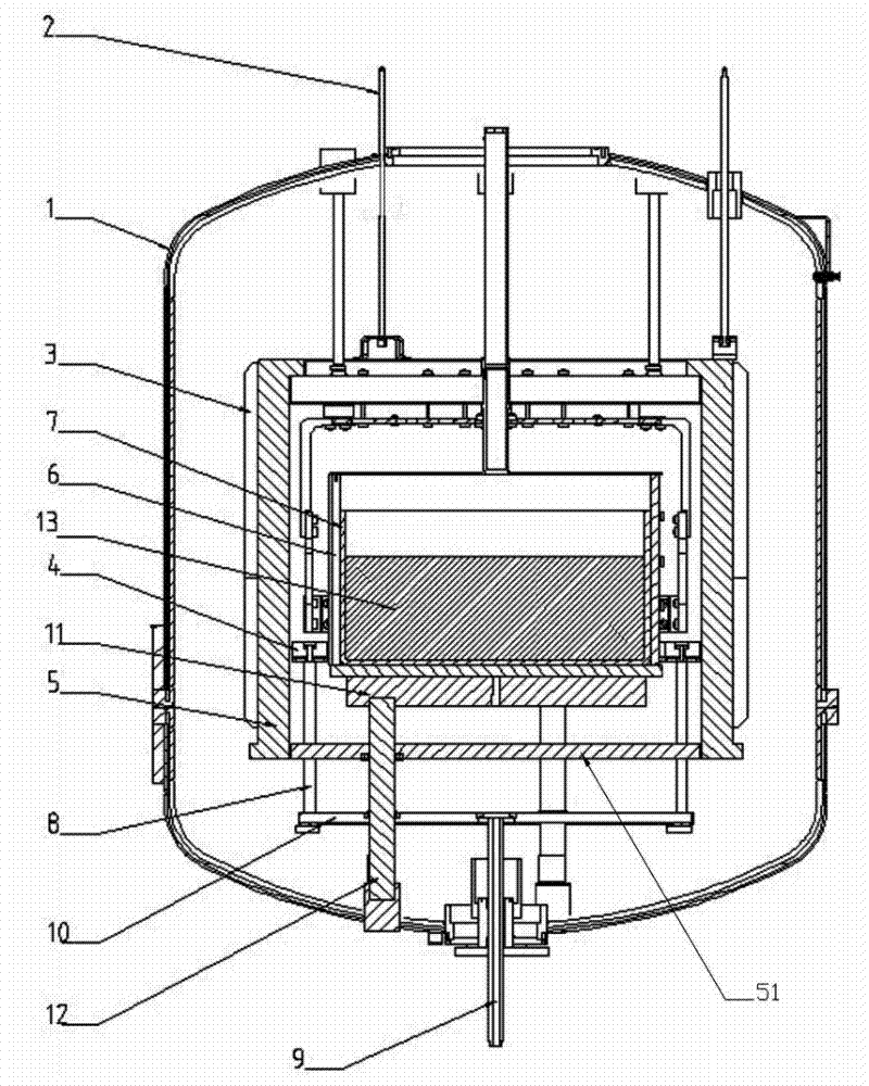
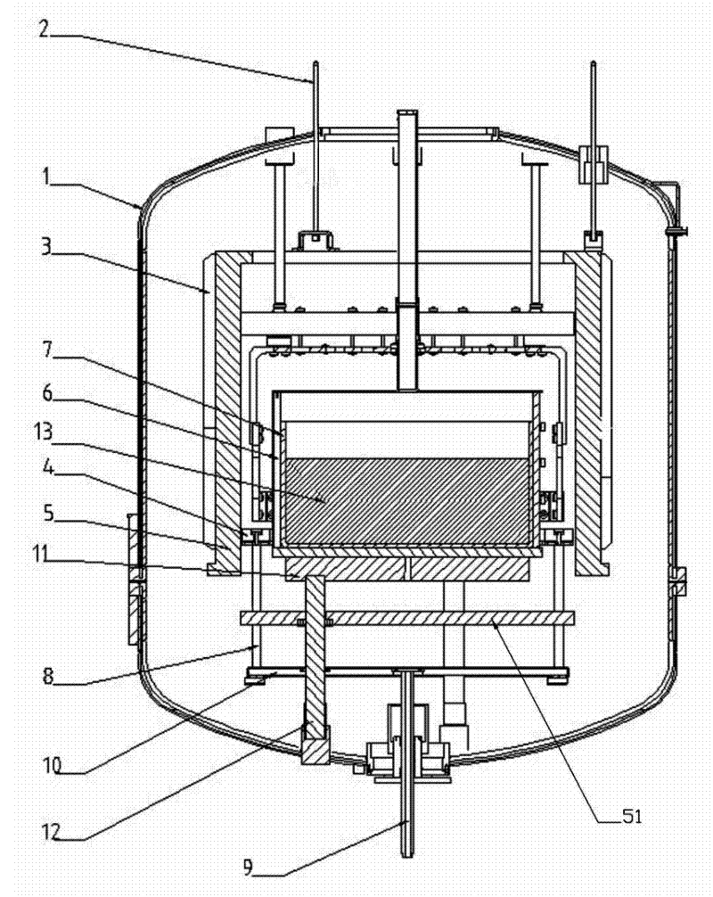
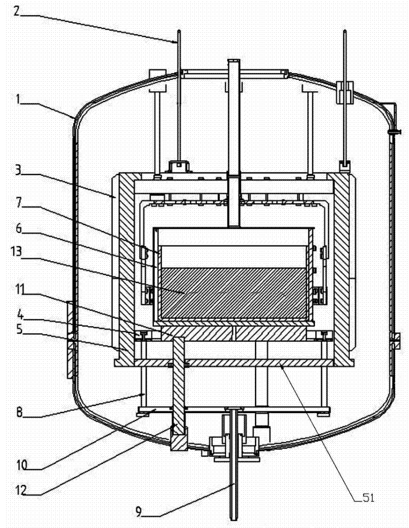
[0027] The bottom lifting device (9) is fixed on the bottom of the furnace body (1), and its main function is to drive the thermal insulation ring (4) to move up and down to protect the seed crystal from being melted.

[0028] The thermal insulation ring strip (4) is composed of four thermal insulation strips fixed on the upper surface of the bottom frame (10), located between the graphite crucible (6) and the thermal insulation board (5), and the initial position is at the same level as the lower end of the graphite crucible (6). Qi is called "zero position" in the industry. The lower end surface of the bottom frame (10) is provided with a lifting rod (8), which is driven up and down by the bottom lifting device (9).

[0029] The silicon material (13) is placed in the quartz crucible (7), the outer layer of the quartz crucible (7) is protected by the graphite crucible (6), and the quartz crucible (7) and the graphite crucible (6) are placed on the heat exchange table (11), T...


PUM


Abstract

The invention provides a manufacturing process of a monocrystalline silicon ingot. The process comprises the following steps: firstly, spraying a layer of seed crystals at the bottom of a quartz crucible, placing a monocrystalline silicon raw material on the seed crystals, and heating for smelting; and then slowly elevating a heat-insulation cage so that heat is diffused out from a heat exchange platform below the heat insulation cage, gradually moving up the height of a solid-liquid critical plane, carrying out upward crystal growth on the silicon material, and then finally forming the solidmonocrystalline silicon ingot, wherein a heat-insulation ring strip is positioned at zero position in the processes of heating and crystal growth and moves downward in the annealing and cooling stages. The invention also provides a thermal field structure of a monocrystalline silicon ingot furnace. The thermal field structure comprises a furnace body, the quartz crucible, a top elevating device, the heat-insulation cage, a heating device, an insulation furnace, the exchange platform and a bottom elevating device. The manufacturing process has the characteristics that the crystal growth of thesilicon material is completed by controlling the elevating speed of the heat-insulation cage; and through elevating and descending the heat-insulation ring strip, solid seed crystals are protected, and the uniform annealing of the whole ingot is ensured. The manufacturing process has the advantages that a large-capacity monocrystalline silicon ingot can be obtained, the yield of the monocrystalline silicon ingot is increased, and the photoelectric conversion efficiency of a silicon sheet is improved.

Description

technical field [0001] The invention relates to the technical field of crystal growth in the photovoltaic industry, in particular to a manufacturing process of monocrystalline silicon ingots and a thermal field structure of an ingot furnace. Background technique [0002] With the increasing application of solar cells, the demand for silicon materials is also increasing, including Czochralski monocrystalline silicon, thin film amorphous silicon, cast polycrystalline silicon, ribbon polycrystalline silicon and thin film polycrystalline silicon, each with its own advantages. Disadvantages: Czochralski monocrystalline silicon and cast polycrystalline silicon are the most widely used at present, accounting for about 80% of solar photovoltaic materials. [0003] In comparison, the conversion rate of monocrystalline silicon is higher than that of polycrystalline silicon. The conversion rate of commercial monocrystalline silicon cells is about 17% to 18%. The current method of prepa...

Claims


Application Information

Patent Timeline
IPC IPC(8): C30B11/00C30B29/06
Inventor 金越顺朱卫峰卫国军袁华均傅建根
Owner ZHEJIANG JINGGONG NEW ENERGY
Why Eureka
Try Eureka