

Method for manufacturing thin film transistor based on anodic oxidation insulating layer
A technology for oxidizing insulating layers and thin-film transistors, which is applied in semiconductor/solid-state device manufacturing, electrical components, circuits, etc. It can solve the problems of low conductivity and difficulty in meeting the needs of large-area preparation, and achieve low preparation temperature and suppression of hillocks. Good growth and uniformity
- Summary
- Abstract
- Description
- Claims
- Application Information
AI Technical Summary
Problems solved by technology
Method used
Image

Examples
Embodiment 1
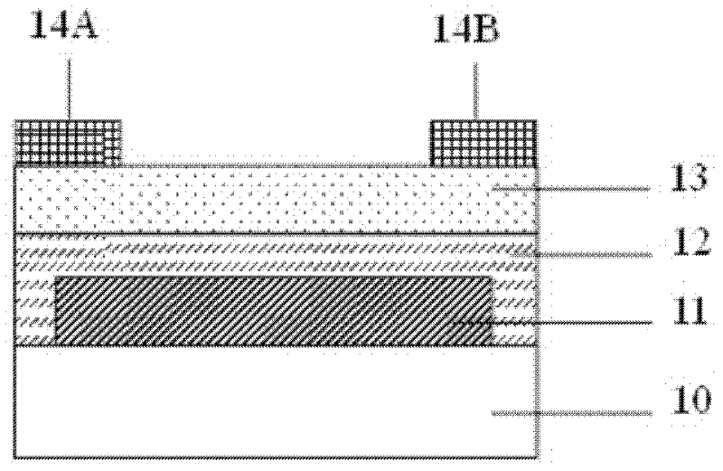
[0047] In this embodiment, a thin-film transistor (a schematic diagram of its structure is shown in Figure 1A shown).
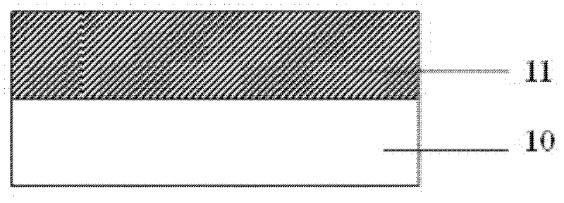
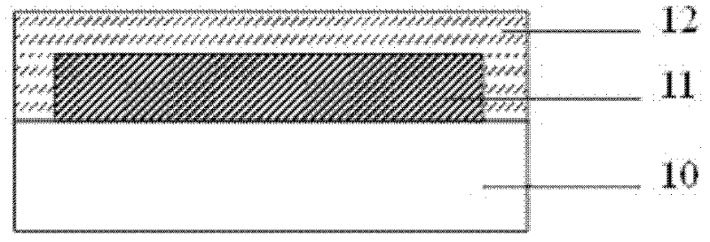
[0048] Wherein, the material of the glass substrate 10 is alkali-free glass with a thickness of 0.4 mm;
[0049] The material of the gate 11 is Al x Nd y (x=0.99, y=0.01), prepared by sputtering, the background vacuum of sputtering is better than 1×10 -3 Pa, argon gas pressure is 0.6Pa, power is 10W / cm 2 , with a thickness of 300nm, formed by photolithography;
[0050] The single oxidized insulating layer 12 is prepared by anodic oxidation. The electrolyte solution used in the anodic oxidation can be a mixture of ammonium tartrate and ethylene glycol. Put the prepared grid 11 substrate and stainless steel plate into the electrolyte solution as the anode respectively. and cathode, first apply a constant current of 0.1mA / cm between the anode and the cathode 2 , the voltage between the anode and the cathode will increase linearly with time, when the voltag...
Embodiment 2
[0055] In this embodiment, a thin-film transistor (a schematic diagram of its structure is shown in Figure 1A shown).
[0056] Wherein, the material of the glass substrate 10 is alkali-free glass with a thickness of 0.4mm;
[0057] The material of the gate 11 is Al x Nd y (x=0.97, y=0.03), prepared by sputtering, the background vacuum of sputtering is better than 1×10 -3 Pa, argon gas pressure is 0.6Pa, power is 10W / cm 2 , with a thickness of 300nm, formed by photolithography;
[0058] The single oxidized insulating layer 12 is prepared by anodic oxidation. The electrolyte solution used in the anodic oxidation can be a mixture of ammonium tartrate and ethylene glycol. Put the prepared grid 11 substrate and stainless steel plate into the electrolyte solution as the anode respectively. and cathode, first apply a constant current of 0.1mA / cm between the anode and the cathode 2 , the voltage between the anode and the cathode will increase linearly with time, when the voltage...
Embodiment 3
[0063] In this embodiment, a thin-film transistor (a schematic diagram of its structure is shown in Figure 1A shown).
[0064]Wherein, the material of the glass substrate 10 is alkali-free glass with a thickness of 0.4mm;
[0065] The material of the gate 11 is Al x Nd y (x=0.9, y=0.1), prepared by sputtering, the background vacuum of sputtering is better than 1×10 -3 Pa, argon gas pressure is 0.6Pa, power is 10W / cm 2 , with a thickness of 300nm, formed by photolithography;
[0066] The single oxidized insulating layer 12 is prepared by anodic oxidation. The electrolyte solution used in the anodic oxidation can be a mixture of ammonium tartrate and ethylene glycol. Put the prepared grid 11 substrate and stainless steel plate into the electrolyte solution as the anode respectively. and cathode, first apply a constant current of 0.1mA / cm between the anode and the cathode 2 , the voltage between the anode and the cathode will increase linearly with time, when the voltage re...
PUM
 Abstract
Description
Claims
Application Information