

Cleaning solution for photoresist
A cleaning solution and photoresist technology, applied in the field of cleaning solution, can solve the problems of strong corrosiveness and insufficient cleaning ability of semiconductor wafer patterns and substrates, and achieve the effects of being beneficial to protection, improving removal ability, and improving solubility
Active Publication Date: 2012-02-01
宁波安集微电子科技有限公司
View PDF9 Cites 15 Cited by
- Summary
- Abstract
- Description
- Claims
- Application Information
AI Technical Summary
Problems solved by technology
[0006] The technical problem to be solved by the present invention is to provide a method for cleaning thick-film photoresist in view of the insufficient cleaning ability of existing thick-film photoresist cleaning solutions or the defects of strong corrosion to semiconductor wafer patterns and substrates. Highly capable photoresist cleaner with low corrosiveness to semiconductor wafer patterns and substrates
Method used
View moreImage
Smart ImageViewing Examples

Examples
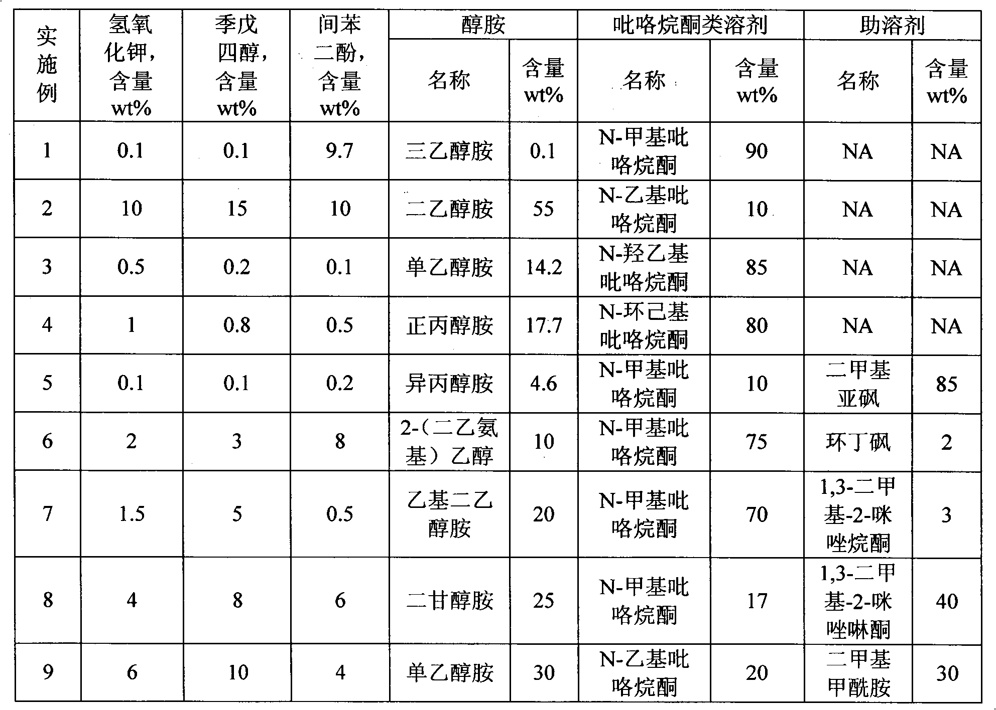
Embodiment 1~27
[0022] Table 1 shows Examples 1-27 of the present invention which are applicable to cleaning solutions for thicker photoresists. According to the formula in the table, each component is mixed evenly to prepare the cleaning solutions of each embodiment.
[0023] Table 1 Components and contents of Examples 1 to 27 of the present invention
[0024]
[0025]
[0026] Note: NA means that this component was not added.
Login to View More PUM
 Abstract
The invention discloses a low etching cleaning solution for removing a thick photoresist. The low etching cleaning solution for a photoresist comprises (a) potassium hydroxide, (b) a pyrrolidone solvent, (c) pentaerythritol, (d)?alcohol amine, and (e) resorcinol. The low etching cleaning solution for a photoresist can be used for removing a photoresist and other residues on a metal, metal alloy or dielectric substrate, and also shows a low etching rate to Cu and other metals, thus boasting good application prospects in semiconductor wafer cleaning and other microelectronic fields.
Description
technical field [0001] The invention relates to a cleaning solution in semiconductor technology, in particular to a cleaning solution for thick photoresist. Background technique [0002] In the usual semiconductor manufacturing process, a photoresist mask is formed on the surface of silicon dioxide, Cu (copper) and other metals and low-k materials, and the pattern is transferred after exposure. After the required circuit pattern is obtained, the Before the next process, the residual photoresist needs to be stripped off. For example, in the wafer microsphere implantation process (bumping technology), photoresist is required to form a mask, and the mask also needs to be removed after microspheres are successfully implanted, but because the photoresist is relatively thick, it is often difficult to completely remove it. more difficult. The more common methods to improve the removal effect are to extend the soaking time, increase the soaking temperature and use more aggressive ...
Claims
Login to View More Application Information
Patent Timeline
 Patent Type & AuthorityApplications(China)
IPC IPC(8): G03F7/42
CPCC11D7/261C11D7/3218C11D7/5013H01L21/31133C11D7/3281C23F1/34H01L21/02057C11D7/06C11D11/0047G03F7/425C11D2111/22
Inventor刘兵彭洪修孙广胜
Owner宁波安集微电子科技有限公司