Two-dimensional photonic crystal laser and manufacturing method

A technology of two-dimensional photonic crystals and manufacturing methods, which is applied in the direction of semiconductor lasers, lasers, phonon exciters, etc., can solve the problems of reduced resonator performance, incomplete refractive index periodic structure, and hole shape changes, etc., to improve freedom degree of effect

Inactive Publication Date: 2012-02-08
KYOTO UNIV +1
View PDF2 Cites 6 Cited by
  • Summary
  • Abstract
  • Description
  • Claims
  • Application Information

AI Technical Summary

Problems solved by technology

[0012] Furthermore, in the method (i), when the upper layer is epitaxially grown, the holes are filled with the material of the upper layer to the bottom, and there is a problem that the shape of the holes changes.
In addition, for the methods (ii) and (iii), it is difficult to completely fill the cavity or between the columnar different refractive index regions with the mater

Method used


Image

  • Two-dimensional photonic crystal laser and manufacturing method
  • Two-dimensional photonic crystal laser and manufacturing method
  • Two-dimensional photonic crystal laser and manufacturing method

Examples


Embodiment 1

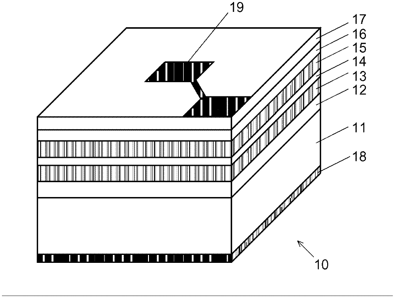
[0110] The two-dimensional photonic crystal laser 10 of embodiment 1 is as figure 1 As shown, a first cladding layer 12, an active layer 13, a carrier blocking layer 14, a two-dimensional photonic crystal layer 15, a second cladding layer (epitaxial growth layer) 16, and a contact layer are sequentially stacked on a substrate 11. 17 structures. In addition, a lower electrode 18 is provided under the substrate 11 , and an upper electrode 19 is provided on the contact layer 17 .

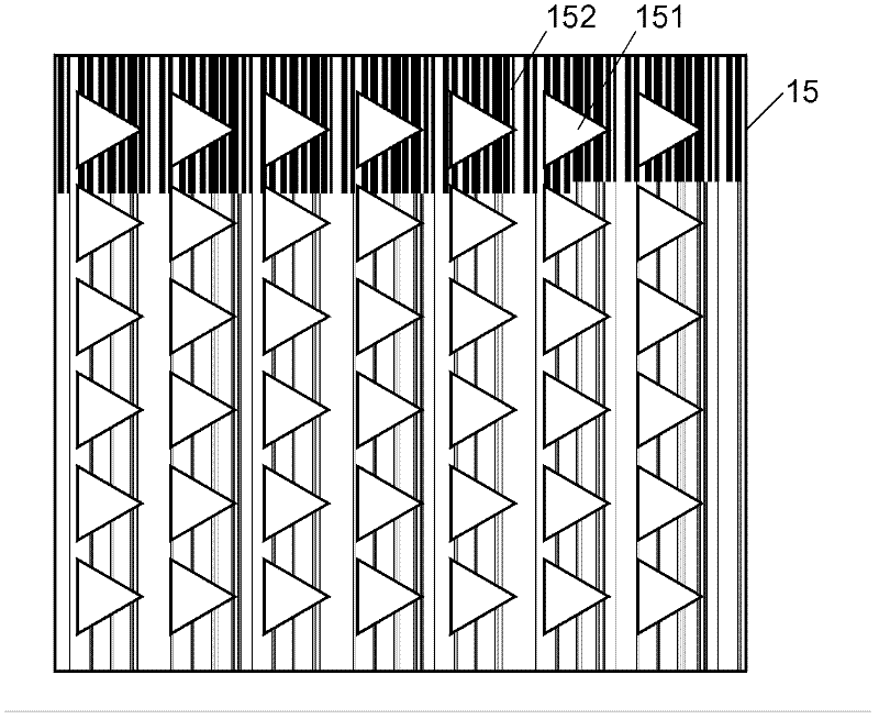
[0111] Two-dimensional photonic crystal layer 15 such as figure 2 As shown, cavities 151 having a planar shape such as a circle or a triangle are periodically formed in the plate-shaped base material layer 152 . In this embodiment, Al is used as the material of the base material layer 152 0.1 Ga 0.9 As. This is because this material is strong even at high temperatures, and the shape of the holes 151 will not be damaged even if the temperature is raised when the second cladding layer 16 is formed ...

Embodiment 2

[0120] use Figure 4 , Embodiment 2 of the two-dimensional photonic crystal laser of the present invention will be described. The two-dimensional photonic crystal laser 10A of this embodiment uses a two-dimensional photonic crystal layer 15A described below instead of the two-dimensional photonic crystal layer 15 of the first embodiment. Other configurations are the same as those of the two-dimensional photonic crystal laser 10 of the first embodiment.

[0121] The two-dimensional photonic crystal layer 15A has Al 0.65 Ga 0.35 The upper surface of the first base material layer 1521A of As (α=0.65) is thinner than that of the first base material layer 1521A. 0.1 Ga 0.9 The base material layer 152A having a two-layer structure of the second base material layer 1522A of As (α=0.1). In the base material layer 152A, the cavities 151A are formed in the same shape and period as in the first embodiment. The second base material layer 1522A has a lower Al content than the first b...

Embodiment 3

[0126] use Image 6 , Embodiment 3 of the two-dimensional photonic crystal laser of the present invention will be described. The two-dimensional photonic crystal laser 10B of the present embodiment is produced by using the two-dimensional photonic crystal laser manufacturing method of the first embodiment.

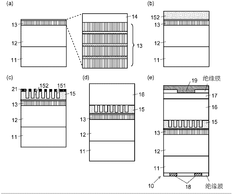
[0127] In the two-dimensional photonic crystal laser 10B, between the two-dimensional photonic crystal layer 15 and the second cladding layer 16 of Embodiment 1, a x Ga 1-x Re-grow interface layer 31 of As (0.4≦x Figure 7 ). For example, when the planar shape of the cavity 151 is a circle, the diameter corresponds to the maximum width; in the case of a regular triangle, the side length corresponds to the maximum width; The side length of the longest side is equal to the maximum width.

[0128] In this embodiment, by setting the Al content x of the regrown interface layer 31 to a relatively high value and setting the aspect ratio h / d to 1.3 or more, the raw material gas...


PUM


Abstract

A two-dimensional photonic crystal laser according to the present invention includes a two-dimensional photonic crystal layer 15 having a base body made of Al[alpha]Ga1-[alpha]As (0<[alpha]<1) or (Al[beta]Ga1-[beta])[gamma]In1-[gamma]P (0<=[beta]<1, 0<[gamma]<1) with modified refractive index areas (air holes) 151 periodically arranged therein and an epitaxial growth layer 16 created on the two-dimensional photonic crystal layer 15 by an epitaxial method. Since Al[alpha]Ga1-[alpha]As and (Al[beta]Ga1-[beta])[gamma]In1-[gamma]P are solid even at high temperatures, the air holes 151 will not be deformed in the process of creating the epitaxial growth layer 16, so that the performance of the two-dimensional photonic crystal layer 15 as a resonator can be maintained at high levels.

Description

technical field [0001] The present invention relates to a two-dimensional photonic crystal laser having a structure suitable for fabrication using epitaxy and a fabrication method thereof. Background technique [0002] In recent years, new types of lasers using two-dimensional photonic crystals have been developed. The so-called two-dimensional photonic crystal is a crystal in which a periodic structure of refractive index is formed in a plate-shaped base material containing a dielectric. Generally, a region with a different refractive index from the base material is periodically provided in the base material (heteroreflective Rate area) and made. With this periodic structure, Bragg diffraction occurs in the crystal, and an energy band gap appears in the energy of light. In two-dimensional photonic crystal lasers, there are point defects used as resonators by using the band gap effect, and standing waves at the energy band end where the group velocity of light is 0, but bo...

Claims


Application Information

Patent Timeline
IPC IPC(8): H01S5/323
CPCH01S5/1231H01S5/187H01S2301/17H01S5/11H01S5/18316H01S5/18319H01S5/3013
Inventor 野田进坂口拓生长濑和也国师渡宫井英次三浦义胜大西大
Owner KYOTO UNIV
Why Eureka
Try Eureka