Method for manufacturing substrate for semiconductor element, and semiconductor device

A manufacturing method and semiconductor technology, which can be used in semiconductor devices, semiconductor/solid-state device components, electric solid-state devices, etc., and can solve problems such as cost increase

Inactive Publication Date: 2012-02-15
TOPPAN PRINTING CO LTD
View PDF5 Cites 3 Cited by
  • Summary
  • Abstract
  • Description
  • Claims
  • Application Information

AI Technical Summary

Problems solved by technology

[0022] But in the end, the holding member 21 is not needed, so the holding member 21 needs to be removed after the casting process, which will lead to an increase in cost.

Method used


Image

  • Method for manufacturing substrate for semiconductor element, and semiconductor device
  • Method for manufacturing substrate for semiconductor element, and semiconductor device
  • Method for manufacturing substrate for semiconductor element, and semiconductor device

Examples


Embodiment

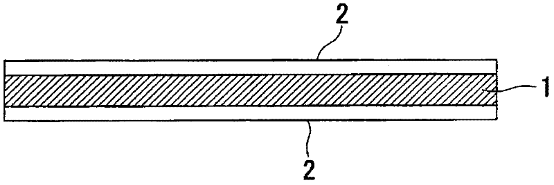
[0062] The size of each manufactured LGA unit is 10 mm per side, and has an array-shaped external connection portion in a plan view of 168 pins. This LGA is stacked on a substrate multiple times, and then cut and cut through the following manufacturing steps to obtain individual LGA-type lead frame-shaped substrates.

[0063] first as Figure 1A As shown, a strip-shaped copper substrate 1 having a width of 150 mm and a thickness of 150 μm was prepared. Then as Figure 1B As shown, a photosensitive protective layer 2 (manufactured by Tokyo Ohka Co., Ltd., OFPR4000) was coated on both sides of the copper substrate 1 by a roll coater so that the thickness of the photosensitive protective layer 2 became 5 μm, and then Pre-bake at 90°C.

[0064] Then, pattern exposure is carried out from both sides through a photomask for pattern exposure having a desired pattern, followed by developing with 1% sodium hydroxide solution, followed by water washing and hard baking, Figure 1C As ...


PUM


Abstract

A method for manufacturing a substrate for a semiconductor element includes: a step of disposing a first photosensitive resin layer on the first surface of a metal board; a step of disposing a second photosensitive resin layer on the second surface of the metal board; a step of forming, on the first surface of the metal board, a first etching mask for forming a connection post; a step of forming, on the second surface of the metal board, a second etching mask for forming a wiring pattern; a step of forming the connection post by etching the first surface of the metal board from the first surface side to a certain point in the metal board; a step of applying, on the etched first surface of the metal board, a resin in the liquid state for pre-molding; a step of forming a pre-mold resin layer by hardening the applied resin in the liquid state for pre-molding; and a step of forming a wiring pattern by etching the second surface of the metal board from the second surface side.

Description

technical field [0001] The present invention relates to a semiconductor element substrate for mounting a semiconductor element. In particular, it relates to a method of manufacturing a lead frame-shaped substrate and a semiconductor device using the substrate. This application claims priority based on Japanese Patent Application No. 2009-064231 for which it applied in Japan on March 17, 2009, and uses the content here. Background technique [0002] Semiconductor elements such as various memories, CMOS, and CPUs manufactured in wafer processing have terminals for electrical connection. The ratio between the pitch of the electrical connection terminals and the pitch of the connection portion on the side of the printed circuit board on which the semiconductor element is mounted differs from several times to hundreds of times in ratio. Therefore, when connecting a semiconductor element and a printed circuit board, an interposer substrate (substrate for semiconductor element mo...

Claims


Application Information

Patent Timeline
Patent Type & Authority Applications(China)
IPC IPC(8): H01L23/50H05K3/40
CPCH01L23/3121H01L23/4951H01L23/49582H01L24/45H01L24/48H01L2224/45144H01L2224/48091H01L2224/48247H01L2224/73265H01L2924/01046H01L2924/01078H01L2924/01079H01L2924/12042H01L2924/15183H01L2924/181H01L2924/00014H01L2924/00015H01L2924/00H01L2924/00012H01L23/28H01L23/48H01L23/50H05K3/40
Inventor 户田顺子马庭进境泰宏塚本健人
Owner TOPPAN PRINTING CO LTD
Why Eureka
Try Eureka