Packaging structure of light source of high power LED

A technology of LED light source and packaging structure, applied in electrical components, electrical solid devices, circuits, etc., can solve the problems of the volume and limited number of thermal conductive columns, and limit the thermal conductivity of the packaging structure, so as to prevent heat accumulation, improve the thermal conductivity, and improve the thermal conductivity. The effect of thermal conductivity

Inactive Publication Date: 2012-03-07
王双喜
View PDF15 Cites 7 Cited by
  • Summary
  • Abstract
  • Description
  • Claims
  • Application Information

AI Technical Summary

Problems solved by technology

The design of the above-mentioned thermal conduction column utilizes the process conditions that LTCC can be printed to improve the thermal conductivity of the low-temperature co-fired ceramic layer, but the volume and number of thermal conduction columns are limited, which limits the further improvement of the thermal conductivity of the package structure

Method used


Image

  • Packaging structure of light source of high power LED
  • Packaging structure of light source of high power LED
  • Packaging structure of light source of high power LED

Examples


Embodiment 1

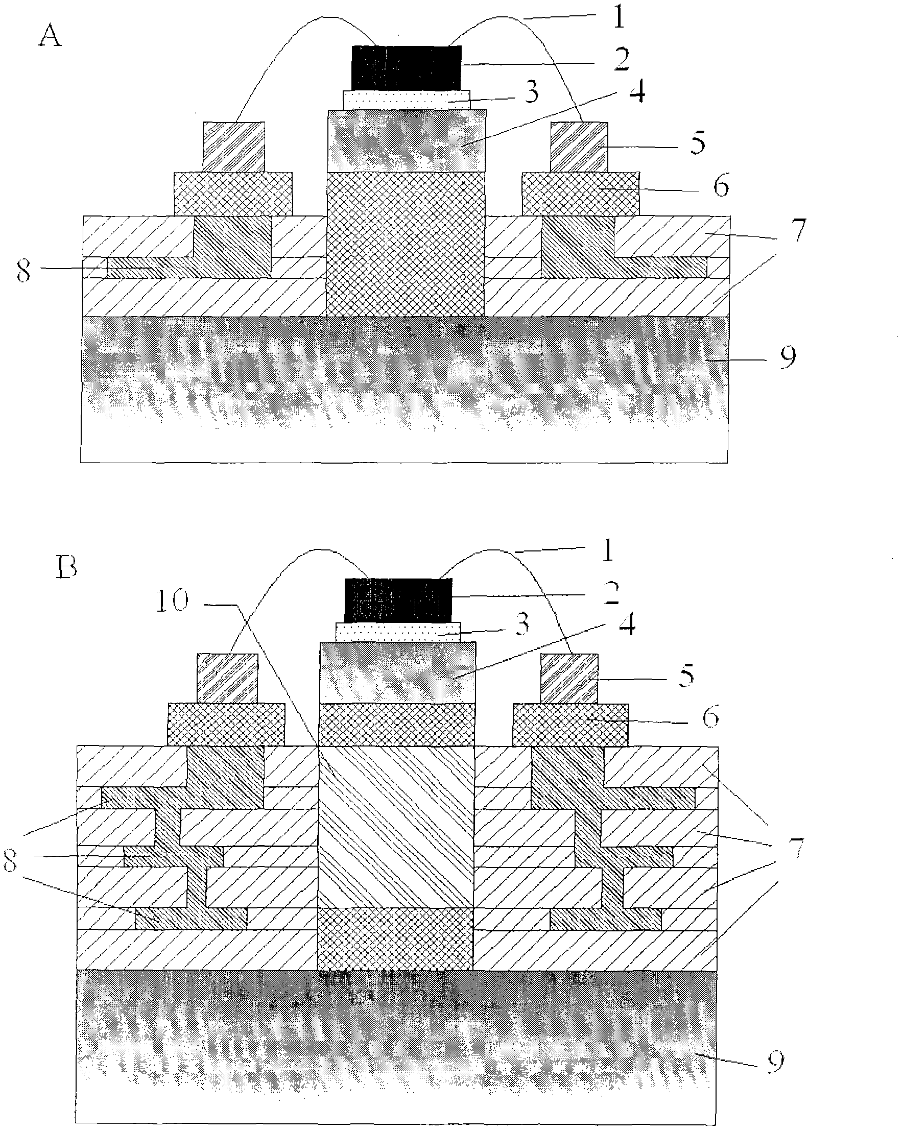
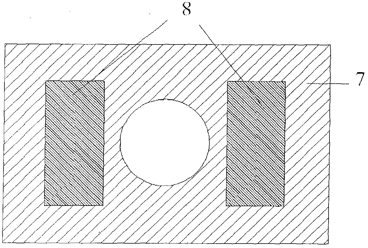
[0025] Such as figure 1 As shown in A, to design a single-layer simple circuit, a total of two layers of LTCC green ceramic sheets (7) are required. Firstly, silver paste of conductive paste (8) is printed on the first layer of ceramic sheet (7) to form a circuit required for design, and a hole is punched in the middle of the ceramic sheet (7) to cut out a heat conduction cavity. Then, superimpose the second layer of LTCC green ceramic sheet (7) on the conductive layer, exposing the electrode position (as attached figure 2 As shown), the second layer of green ceramic sheet is also cut out with the same heat conduction cavity shape as the first layer of ceramic sheet, and co-fired to combine to form an LTCC substrate. The LTCC substrate is closely connected with the metal heat dissipation base (9) and the aluminum alloy substrate with the LED chip through solder (6). At the same time, the electrodes (5) of the LED chip particles are welded on the LTCC substrate through the s...

Embodiment 2

[0027] To design a multi-layer circuit, the number of LTCC layers required increases, and the circuit and heat conduction cavity manufacturing process are as shown in the first embodiment. The axial size of the heat conduction chamber increases, so it is not suitable to use solder to connect the chip particles and the metal heat dissipation base. At this time, a metal heat conductor with a thermal expansion coefficient matching the LTCC material is selected (10) Cu-Mo-Cu alloy is co-fired with the LTCC substrate, and preheated Leave a certain welding position, such as figure 1 As shown in B, the fired LTCC substrate is then welded to the metal heat dissipation base and chip particles.

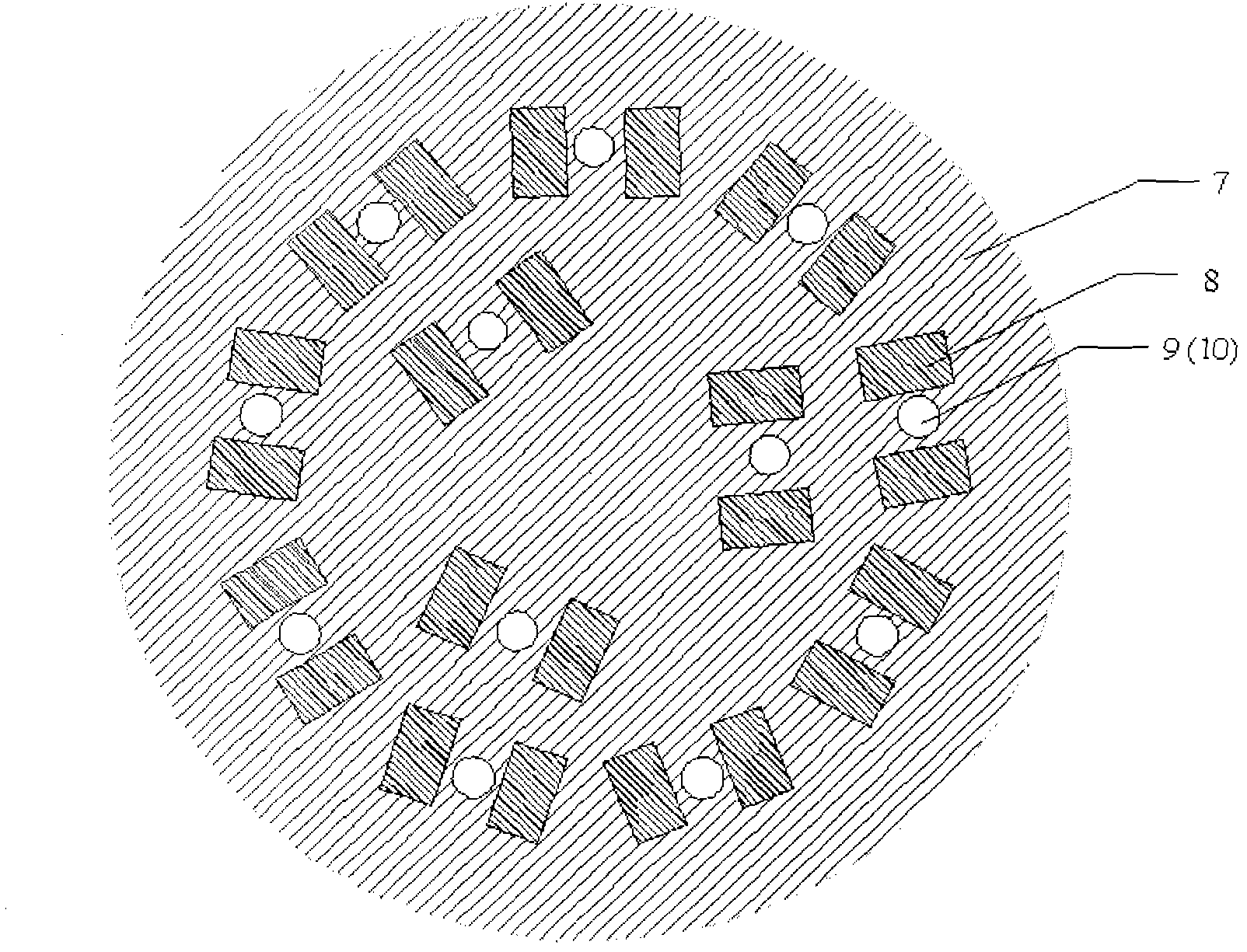
[0028] In this embodiment, the LED array can be designed into different numbers of circular arrangements, rhombus staggered arrangements, etc. according to needs, without limitation.


PUM


Abstract

The invention relates to a packaging structure of a light source of a high power light emitting diode (LED), especially to a packaging structure of a light source of a high power LED, wherein a low temperature co-fired ceramic (LTCC) technology is applied to the packaging structure. The packaging structure comprises a ceramic substrate, an LED chip and a metal heat-dissipating base, wherein the LED chip is fixed on the substrate. According to the invention, the LTCC substrate is a slice; a conductive channel is printed on the slice; and the conductive channel is mutually independent with other electrical conductors. Besides, layers of the LTCC and a circuit layout in the LTCC are set according to a design demand. Moreover, in order to improve a heat conducting property of the structure, a large area of a metal material is employed to enable heat at the bottom of the chip to be rapidly led out to the metal heat-dissipating base. On the whole, the packaging structure provided in the invention is suitable for packaging with high power and multiple chips as well as can be applied to packaging of a three primary color light source and a white light LED light source.

Description

technical field [0001] The invention belongs to the technical field of semiconductor packaging, and mainly relates to the packaging technology of high-power light-emitting diode (Light-Emitting Diode, LED) light source, low temperature co-fired ceramic technology (Low Temperature Co-fired Ceramic, LTCC), and the packaging structure of LED light source. technical background [0002] As the world's most attention-grabbing new-generation light source, LED is known as the most promising green lighting source in the 21st century because of its advantages such as high brightness, low heat, long life, non-toxicity, and recyclability. With the emergence of ultra-bright LEDs, the application of LEDs in various signal display and lighting source fields has been greatly expanded, mainly including automotive interior and exterior lights, traffic lights, lighting, indoor and outdoor information displays and backlights, etc. [0003] The core part of the LED is the PN junction. When the i...

Claims


Application Information

Patent Timeline
Patent Type & Authority Applications(China)
IPC IPC(8): H01L33/48H01L33/64
CPCH01L2224/48091H01L2224/73265H01L2924/00014
Inventor 欧阳雪琼王双喜郑琼娜
Owner 王双喜
Why Eureka
Try Eureka